Need help with identifying this BMS

samsungante

1 µW
Joined
Feb 25, 2021
Messages
3
Basically, I am doing a small portable battery bank out of thesee hoverboard batteries (110Wh) for my school project.
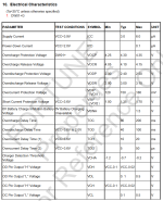
But in my paper I should describe basic principle of operation of every component. I have no clue in power electronics and im stuck at BMS description,
All i know is that there is 7 controlers for every series part.
I see 4 MOSFETS and RS3M diode that connects B7 and P- section. Is there any short circuit protection ?
Please if anybody can regognize anything more in detail on this PCB be welcome to comment.
I have no idea is this 10A or 15A. :(
is there any balancing implemented ? i mean there could be even if there is no resistors for charge bleed, maybe some other type ?

bms opis.jpg

BMS pokraj 7s2p baterije.jpeg
 
Bad BMS many had problems. I have read ( here, on the Sphere,) about the use of the DW01 chip in series applicatins and teh faults associated with such.

Just a heads up. Link to follow. Describing operation.

Link:

Circuit analysis of a cheap BMS, and why you shouldn't use one

https://endless-sphere.com/forums/viewtopic.php?f=3&t=103527&p=1560092&hilit=dw01#p1560092

It is what the EE expert MAXIMUM_AMPS calls a "Chineeseum BMS".

The Fets open/close the main current path. The DW01(s) handle the balance requirements. There is probably a system implemented to limit current on charge and discharge. There are a few ways BMS implement this protection. IDK how that one does explicitly, measure the current and decide as to protect of not. I am not familiar. Maybe someone will be along soon. Tell us more.

1. Each of the protection chips (DW01A) is separate, there is no cooperation. Meaning: one chip could fail, due to ESD, water droplet, etc. Then that cell group is completely unprotected, opening up the possibility that the cell group could become overcharged and explode unexpectedly! With a 2-wire monolithic design, if one part fails, due to ESD, etc, the output FETs are turned off PERMANENTLY. This is much safer, as charge can no longer flow in or out. Crisis averted, while also alerting the user of the failure.

2. For exactly this reason, the manufacturer states clearly that the DW01 is a 1S ONLY protection chip. Using them as a 4S, 10S, 14S, etc is NOT RECOMMENDED because of this safety hazard! That's what t
-MAXIMUM_AMPS

FROM THE DWO1x .pdf

https://www.ic-fortune.com/upload/Download/DW01x-DS-17_EN_53550.pdf
 

Attachments

  • DWO1chip.PNG
    DWO1chip.PNG
    49.3 KB · Views: 179
I see. Well I also tought that there is no much quallity here. Well what can u do, I have what I have. That RS3M diode at the b7 and p- terminal is for short circuit protection or for reverse polarity protection. Those two big R010 resistors are used as current shunt for overcurrent protection ? ... anybody feel free to comment I need as much description on this CHENESIUM BMS xD

anyway i connected 6 of these in paralel (7awg copper paralel bridge ) and was charging them with mpt-7210 "solar" charge controler ...i set up upper voltage of 29.2v (4.17v per cell 7s2p config) that worked well they all have the same voltage after disconnecting and letting them for 2 days unplogged from paralel bridge.
WHAT I would like to add is that after connecting them on the 24v INVERTER when they reached 23 VOLTS inverter suddendly lost power, that is interesting because inverter can go down up to 19.5v ...so my conlusion is that these bms disconnected battery at that voltage of 3.3 or maybe 3.25v ....

if there is no short circuit protection I will add 10amp fuse on + side of every hoverboard battery as a added protection

I AM NOT PULLING ANYTGHING MORE THAN 5 amps FROM every hoverboard battery ... in hoverboards they were powering 250w or possibly 350w motors ...so in my condition they are having as they say "easy living"
also to add that they are all new battery packs never used (had 5years shelf life, company that marketed those hoverboards closed and sell of all of their service parts )
 
If the specs in that datasheet are the right ones for that board, it would trip at 30A.

The BMS measures the current by measuring the voltage across the two shunt resistor near the B- connection. You can change the trip point by changing those resistors. It's not a bad idea to use fuses anyway in case the BMS fails. You want the BMS to trip before your fuse blows, so a 30A fuse. If you removed one of the two shunt resistors, it would trip at 15A.

It does appear to have balancing resistors (100 ohm), which would give around 42mA balancing current. This is pretty typical.

This is a "single port" design, where both charge and discharge go through the same pair of wires.

When it tripped running your inverter, most likely one cell got below the cutoff threshold. Keep in mind that under load, the cell voltages may be a lot lower than when resting. You might try measuring the lowest cell while it's under load.
 
My advice is atomize the packs to re-use just the cells, build a new pack out of the good ones.

Buy a new BMS for your pack selecting it on the basis of clear documentation, not just from the vendor, but from teardown / rebuild discussion threads here and in other forums.

 
I will atomize 6 packs later but for now I just want to finish this project. Can somebody comment me on those 4 big mosfets HY1707...their source is connected short in the middle where they touch...what is their purpuse in a bms ? i understand that they act basically as a switch but is there more to add to that ?

1.dw01 is a ic for series in the battery pack they have those little 105 resistors that goes on the base of those 2l transistors (one for charging one for discharging)
2. 2x 010 shunt resistors are for current sensing
3. RS3M diode is for reverse polarity protection
4.i dont know how to simply describe the role of 4 hy1707 mosfets ???
5. IT seems that there is NO balancing bigger resistors for charge dissipation,..i doubt that job for that task is given to those little tiny resistors on the 2L area
 
Back
Top