eBike Master Switch Design

Alan B

100 GW
Joined
Sep 11, 2010
Messages
7,809
Location
San Francisco Bay Area, USA
News - The V1.0 board is openly available, see the V1.0 page linked at the end of this posting

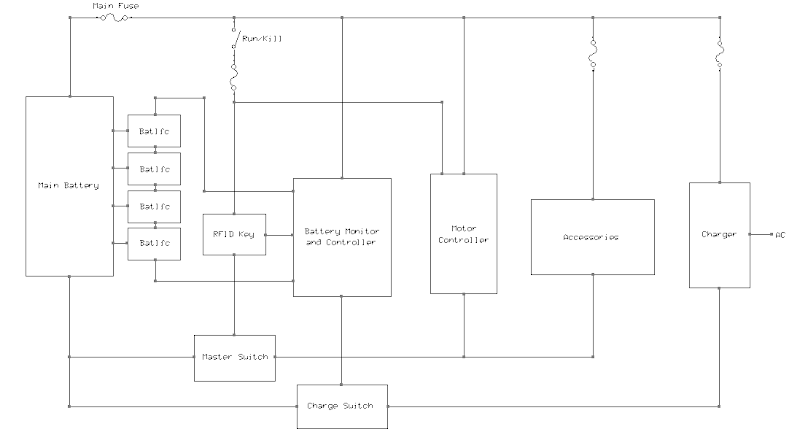
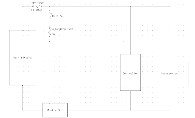
Ebike designs have a variety of ways of handling the "master power switch" covering a range from just using plugs to contactors and electronic switches. On my current Greyborg I used a "Kill" switch that feeds power to the controller and lights while the real master switch is some large PowerPole connectors. I find that the Kill switch is a really nice way to turn the bike on and off, much more convenient than getting to and fighting with the big connectors and precharge resistors or watching your connectors get eaten away by arc-flashes at each hookup.

The downside to this technique is that the bike is still somewhat "on" all the time and the controller is draining the battery slowly even though the logic power is off as the high power section is always energized. Installing a big contactor is not that appealing, but making a small one with FETs is an interesting possibility. A few folks on ES have done similar things, and many BMS systems have an FET switch built into them. In fact this master switch could be used as part of a DIY BMS as well as being the master switch.

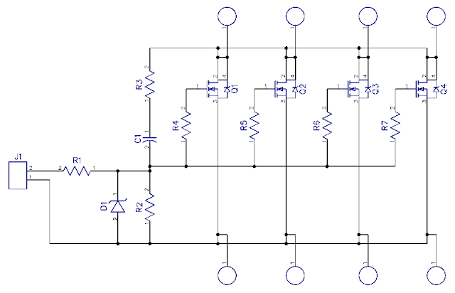
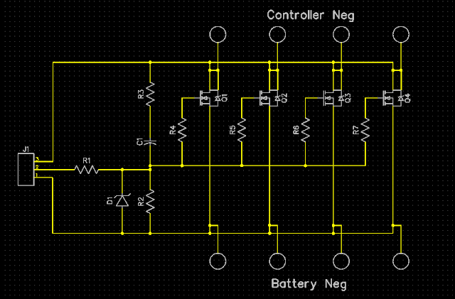
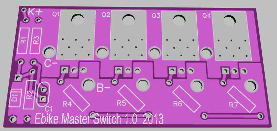
Lately I've been learning a (new to me) PC layout package called DipTrace, so I decided to make a layout for a simple electronic Master Switch. This one has a feedback type soft start and four parallel FETs which should be adequate for a 24 FET controller. If you push your controller hard you might need a heatsink and beefed up traces. Or we could add a couple more FETs easily enough :mrgreen:

ebike%2520master%2520switch%25201.0.png


This design uses four parallel 12 gauge wires to carry the current (equivalent to a six gauge wire!), and to turn it on a single wire to the Kill (or ignition) switch connects to +battery. The current carrying portion of the switch connects between Battery minus and Controller minus. So only three connections. It will draw only about a milliamp when on (to power itself), and when off only the leakage of the big FETs which is typically in the microamps region depending on temperature and FET quality.

If you want to add a keyswitch or hidden switch in addition or in lieu of a Kill switch (though all ebikes should have a standard kill switch) you can add any switches in series and feed this Master Switch board. Later I'll make an RFID ignition switch that will use this board to control the main power (together with the Kill switch).

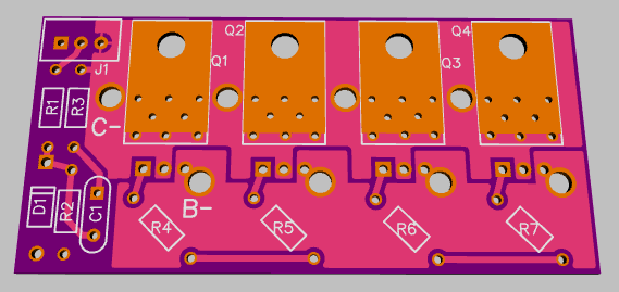
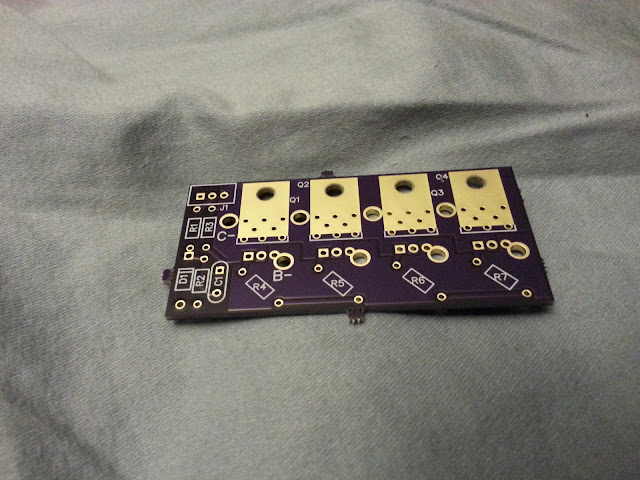
This is an easy to build PC board with all through-hole parts. The FETs are bolted to the PC board to make a solid mechanical unit so vibration won't break the leads. If it is of interest to other folks we might be able to make extra boards.

Updates, index here:

V1.0 board info post: http://endless-sphere.com/forums/viewtopic.php?f=14&t=54225&p=808093#p808093 This board is available at OSH Park, there is a link in the page to order them.

V1.1 board info post: http://endless-sphere.com/forums/viewtopic.php?f=14&t=54225&p=825100#p825100
 
You using a resistive divider for the gate charge? I've been running the same sort of circuit for about a month now using a few stacked TO-247s.
 
Try them out first. I had trouble running resistor divider board for high power controller. I plan to the other circuit fecther recommend. The one with diodes and capacitors.
 
Interesting, I hadn't noted Fechter's recent material on this topic. I did some searching but hard to know when you don't find something.

I did this circuit design some time back (over two years ago), it is very similar to Richard's in using a feedback capacitor to slow the turn-on ramp way down. I discussed it with Jeremy on his RFID switch thread (over a year ago) and he didn't think it was necessary, but his packs were lower voltage and higher impedance.

The circuit is very simple, the challenge here is to get enough current carrying capacity, pc boards are not great at that. I'm making adjustments to this design to reduce the heating in the PC board. One advantage of TO-220 parts is the large contact area for the drain on the back, the TO-247's are generally insulated there. They do have better leads, but you lose that big metal tab to connect to.

Luke was making thin copper layers that could be added to the high current traces of a PC board, that's one way to beef this up. It is easy to add a heatsink across the tops of the TO-220 tabs, or under the TO-220's against the PC board.
 
Ebike System Diagram with Master Switch

Ebike%2520Master%2520Switch%2520System%2520Diagram.png


The important detail here is when the kill switch is turned off (opened) the Controller loses power right away so it won't continue to run the motor while the FETs ramp down, which could put a large heatload on them. If the controller's low voltage cutout is set right that will help also in keeping the load down until the FETs are fully saturated.
 
If your power demands are higher you can use two of these Master Switch boards in parallel. :)

Or you can parallel the board with a shorting plug, large switch or contactor and just allow the board to do the pre-charging and lower power operation. The Kill switch would still work by turning the controller off.

It will take actual testing to find out how much current these will handle before they get hot, and it depends on the FETs that you mount on the board.
 
Yeah the best thing is to leave the traces without solder mask and beef up the traces with wires for higher current. Those traces on the PCB is definitely not enough to sustain anything higher than 20A. And even 20A is a bit optimistic.

I was building something similar. Going on jeremy's design, I did not get it to work and some people had similar problems of blown FETs.

I think there has been more luck with fetcher's design using higher power controller.

But great design! Though personally I would go with surface mounts just to make it cleaner/compact. But that is just me.

Here is an excel sheet which I made to figure out how many FETs are required for certain current draw and how which FETs to use.
https://docs.google.com/spreadsheet...hTWlRKelptR0VxUWVFUHZTV1E&usp=drive_web#gid=9

Depending on what voltage you want to run, different FETs are better than others.

Just for reference, here is the other thread discussing this topic.

http://endless-sphere.com/forums/viewtopic.php?f=3&t=40142&start=100
 
nicobie said:
We really need a switch like this. I hope yours works!

I had high hopes for Method's switch, but it seem that he has lost interest in everything. :cry:

There was also an attempt from someone else but it never got to the point where he could sell them.

Subscribed!
 
Hmmm - Analog design is far from my forte, but unlike logic switching applications, doesn't the intentional slow turn-on nature of this circuit make the gate resistors superfluous? Also, although there are paralleled FETs, the matter of limiting/balancing gate turn-on currents to balance thermal load also does not appear to be a design consideration. I was wondering if you might help clarify this a bit. (Just wondering if these components can't be eliminated and the board reduced in size a bit.) Thanks!
 
Thanks for the feedback folks, we'll have to see how this works. I made a circuit board with this design awhile back and arranged for someone to test it but it never happened, and I didn't get around to testing it myself either. :(

I made a LOT of changes this morning to get the schematic and layout to fully agree (in fine details like pad layouts, etc), and to better fit the capacitor spacing.

On the question of gate resistors, I don't think they are necessary here either, but I included them partly to keep the copper pour clean near the FETs, and allow experimentation in case there is some value during the ramp (which I don't see at this point either). We could eliminate them, but it would cut into the copper right where we need it most. The circuit board needs to be big enough to dissipate the heat, so making it too small might be a problem.

I'm employing every trick I can think of to help this PCB handle lots of current without going to extra-heavy copper. I want to make it do the best I can without that, we can always do that later at greater expense. If you look at the board closely you'll see that a lot of thought has gone into parallel paths and wide traces/pours and very short paths for the high current. Four 12 gauge wires bring current on and another four bring it off the board, and these wires are positioned very close to where the current needs to go. On the Source side the wire and the FET lead are basically almost touching, and on the Drain side the wire is almost touching the TO-220 thermal pad which is also electrically connected to the drain. So the actual distance the current traverses the board is very small, and yet there is lots of copper to conduct away the heat generated by that little jump on PCB material. There are also traces on both sides in every case. Still, it will overheat at some level, the question is at what level?

I'll look into clearing the solder mask, I'm not sure how to do that yet in DipTrace.

I did this design through-hole because I want it to be buildable by anyone (and circuit boards and SMT parts aren't so great at these current levels). It is going to be hard to solder with all that copper, but we need that.

OSH Park has a feature where you can share circuit board designs, anyone can have boards made. I'm considering putting this one in the library there when it checks out, then it would be a resource for all.

If it gets hot we have lots of ways to improve it, they are just not as easy as the circuit board is to make.

I'll get three of these prototype boards about 2-3 weeks after I order them (which should be in the next day or so if I stop making changes). If anyone wants to participate in testing one of them I'll consider it, drop me a PM but ONLY if you're really serious and have the time and equipment to test it. You'll have to provide your own parts. It may fail in any number of ways, that's what we're setting out to learn. I've got a lot of hours in this design and layout, and I've spice modeled the turn-on (and Richard measured his so there's some actual data on that), but I'm not set up to model the thermal behavior. We've got some experimenting to do!
 
I was going to put up another render this morning but didn't get to, the one above is larger than the present one, and the current carrying wires have been moved closer to where the current is coming from or going to, the resistors downsized and the whole board shrunk vertically perhaps 20 percent, now there isn't enough room for the board description on the top, so I had to move that to the solder side. :)

Perhaps tonite I'll do another rendering to here, maybe the final prototype version.
 
I expanded the system diagram to include some future elements and found a new requirement for the Master Switch, so I'll have to add one more conductor to the connector on there, very easy to do. This will minimize future cabling in the system, one of my overall goals.

Ebike%2520Power%2520System%2520Drawing.png


I see how to eliminate one more cable, but it does not affect the Master Switch board.
 
This page has been updated to contain all info about the eBike Master Switch Rev0 PC board.

The Rev1 board is here: http://endless-sphere.com/forums/viewtopic.php?f=14&t=54225&p=825100#p825100

This Rev0 board is simpler and adequate for most uses. The PC Board is available, see the bottom of this posting.

Rendering:

ebike%2520master%2520switch%25201.0b.png


Photo of the actual boards from OSH Park (one of three):

2013-10-26%252022.38.46.jpg


Depending on your monitor the above may be larger than life. :)

Thermal Vias are not supported in DipTrace currently. This is not fun to workaround, or pretty.

BOM (default values, see table below for alternates)

R1,*R2 100K (all resistors 1/4W through-hole type)
R3 1K
R4,5,6,7 shorting jumper or 1K
D1 12-15V Zener
C1 1uF ceramic, rated voltage at least 1.5x your maximum battery voltage
Q1,2,3,4 TO220 Power Fet, same as is in controller or similar (should be bolted tight to PC board with a trace of thermal paste under or the tab fully soldered to the board)
J1 3 pin JST-XH (or wires)

Default values are chosen to operate over a wide range of voltages, the downside is that turning off occurs several seconds after turning switch off.
*R2 values for optimizing turn-off times are voltage dependent, see the following table:

Code:
   R1	 R2	C1  Vth	Batt ON    OFF    Vgate
	k	  k	 uF  V	  V    mS	 mS	  V
	100	100  1	3.5	100  104	2857   50  default values have slow turnoff
	100	10	1	3.5	100  104	286	 9
	100	12	1	3.5	75	105	257	 8
	100	22	1	3.5	48	108	302	 9
	100	27	1	3.5	36	111	278	 8
	100	47	1	3.5	24	117	322	 8

Note that with the large capacitor banks that most controllers have, turn-off is not instant with any switch unless the motor (or something) is drawing power. It takes awhile for the energy in the capacitors to dissipate.

Schematic for this board is below, in this posting.

J1 pin 1 [square pad] Battery negative (B-) (does not need to be connected)
J1 pin 2 control, switch to Battery or Controller positive to turn on (needs to be connected for turn-on)
J1 pin 3 Controller negative (C-) (does not need to be connected)

Battery and Controller wiring:

For max rating use 4 each #12 stranded wires the same length from each board hole to the joining connection offboard, meeting in a good connector (such as PowerPole 75 which will take 4 #12 wires).

Make sure not to mix the wires up:

"B-" connections (4) go to negative battery, 4 wire connections, nothing aside from this switch board and charger should connect to this circuit
"C-" connections (4) go to controller negative, 4 wire connections, all loads should connect to this circuit for negative

NOTE that if a remote switch is not wanted you can connect J1 pin 2 to controller plus, and then when power is plugged in it will ramp, making a nonsparking connection with the battery possible.

NOTE that less than 4 FETs may be used if the current is lower, consult spreadsheets above for some guidance and watch temperatures in use. The number of wires used should correspond to the number of FETs for best current handling capacity a wire should be coming in and going out of each used FET position.

WARNING - Exposed high DC voltages are present on this board, whether ON or OFF the battery negative and positive voltages will be present on the FETs and other components. DO NOT TOUCH when connected to the battery!! PROTECT from fingers when mounted on the bike! :shock:

WARNING - AVOID turning the throttle until voltage has ramped to the full system value. Doing so will dissipate a lot of power in the FET switch and may cause it to overheat and fail. Setting the controller's minimum voltage to a proper high level may help to protect against this.

Schematics:

Ebike%2520Master%2520Switch%2520PCB%2520Schematic%2520I%2520b.png


Recommended System Diagram:

Ebike%2520Master%2520Switch%2520System%2520Diagram.png


Get PC Boards:
badge-5b7ec47045b78aef6eb9d83b3bac6b1920de805e9a0c227658eac6e19a045b9c.png

https://oshpark.com/shared_projects/DnDUyD6D
OSH Park allows inexpensive ordering in multiples of 3 pc boards.
 
This is a great idea, I just cooked my master power switch this weekend. Forgot to pre-charge one too many times and it welded itself closed. It was a 30A rated heavy duty toggle switch and I'm running a 25A controller, but inrush current vastly exceeds 30A, obviously, and it just couldn't take it. I could hear the arc welding happening inside.

So I'll totally buy a couple boards if you make some of these.
 
Alan B said:
Ebike Master Switch Schematic

Ebike%2520Master%2520Switch%2520PCB%2520Schematic.png
As an analog designer, the way this works:

R1 with R2 devide down the jumper J1 voltage so something less than the 20V FET gate limit.
The battery with the resistors makes an equivalent voltage source (V_eq) of V_j1*R2/(R1+R2)
The equivalent resistor (R_eq) is R1*R2/(R1+R2)'.

knowing this, and the threshold or turn-on gate voltage of the FETs (V_t) you can calculate
the turn-on time.

At start capacitor C1 is charged to the battery voltage. When the key is turned this cap is
discharged by a current (V_eq - V_t) / R_eq, the voltage across the cap follows the standard
I = C *delta_V/delta_t equitation. So, the voltage across the controller will rise linearly.
Using this slope, and the size of the caps in the controller, you can calculate the (FET) current
it pulls during the switching event.

R3 is probably there to prevent the FETs from blowing up when the main battery is connected.
The gate resistors serve no real function.
 
Alan B said:
Nice analysis Lebowski.

I plan to use 1 meg for R1 and R2 so the Zener will determine gate voltage maximum at 12-15 volts, R2 is more to drain the gates than as a divider. I don't like floating gates.

Then the current charging C1 will (roughly) be (V_j1 - V_t)/R1
 
Back
Top