zombiess
10 MW
We have several designs going on in this forum so I'll share some troubleshooting tips which hopefully aid in the design/construction. There are many issues which crop up when paralleling devices, most of them tie back to layout issues and parasitic inductance.
For more details on this topic I suggest you read this paper by Toshiba on paralleling devices. It does a good job describing resonance issues and matching Vgs_th. I researched this technique several years ago when there was hardly any info available, nice to see this paper do a good job at describing it. I'm not advocating to match your devices as it's not favorable to manufacturing in large quantities, but it's something you should be aware of.
https://toshiba.semicon-storage.com/info/docget.jsp?did=59458&prodName=TK8P65W
These scope shots are from 5 paralleled IRFP4568 devices on the low side and 4 of them paralleled on the high side (the difference is due to other testing I was doing). This is ~30V DC on the bus at 60-80A pulses into a either a 5uH or 20uH coil (not sure which).
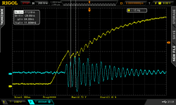
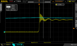
Here is an example of a turn on ringing issue:
The below scope shot shows the G-S voltage (yellow) vs G-S current (blue). This ringing you see is very common in parallel arrangements and is typically caused by issues in the layout of the gate traces. The parallel MOSFETs end up representing a Colpitts oscillator (see the toshiba PDF for more info). As you can see, as soon as the Vgs reaches the Vgs_th around 6V, the MOSFET turns on. Once it does so, you see that the current into the MOSFET is ringing. This ringing causes the Vgs voltage to also ring because the amplitude of the current is still significant at around 800ma P-P. This is enough current to cause the charge on the effective capacitance at Qg to fluctuate. This Vgs fluctuation is then carried over to Vds and is seen as ringing/spikes. What is happening is there is an excitation of the parasitic inductive loop formed by the G-S of the devices and the gate traces. Ta daa! Oscillator.
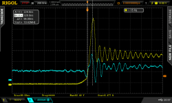
Below is what gate current it looks like at turn off. How quickly the device is switched is akin to striking a gong with hammer. It's always at the same frequency, but how loud it rings is related to how hard it was hit. Looking at some other shots in my notes, it appears I was switching the device on/off (referenced drain to source) in about ~250ns, aka way to fast, but this was bench testing to investigate and tune this issue out so I was trying to excite it.
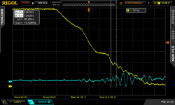
Here is the Vds vs Ags at turn off: Look at all that ringing, and this isn't even that bad, but it shows you how improper design/ layout on the gate drive traces will muck things up. This is your traditional turn off overshoot + ringing issue. The first step to mitigate the issue is to slow down your transition times by increasing your gate resistor.
In this shot it appears I had already made some adjustments to the layout / switch speed as can be seen by the lower amplitude and duration in the Ags ringing at turn off, but it shows what is happening with the gate current. Also of note is the change in slope at turn off, this gate driver was using a 2 level turn off circuit. I probably had the miller clamp engaged as well, using a miller clamp helps to kill off the resonance in the gate traces by tying them to their respective grounds forming a low impedance circuit.
So far I've shown you the results of issues of ringing on the gate driver traces, but there is also ringing which happens due to the power pass sections layout inductance.
It's common for designers to try and slap a bunch of capacitance on their DC bus layout throughout a design in an attempt to reduce turn off overshoot. Sometimes it works, sometimes not, there are many variables at play. Slapping additional caps of any kind into a resonant circuit and calling it good is a bad design practice, but there isn't a much good info out there on this topic.
This is a shot before adding additional capacitance to the bus bar. As you can see, it has a large overshoot at turn off, at least 30V over the 30V DC bus, followed by about 5us of quickly decaying ring.
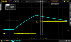
Enter what many designers try to do, add additional capacitance to the DC bus. In this case an additional 1uF polypropylene cap was added. Looks like it worked, overshot dropped from just over 60V down to around 55V. You might notice that this shot looks a little different, there is now an excitation of a ~660kHz resonance in addition to the 10MHz ring. This 660kHz is being excited within the DC bus layout, so now there are 3 problems which need to be addressed. Turn off overshoot, gate drive resonance ~10MHz and DC bus resonance 660kHz. As a test, I'd add an additional 10nF G-S capacitance to the gate trace before adding additional caps to the DC bus. This can be done at each individual MOSFET, or as a single additional cap, you need to experiment to see what works best if you go this route.
I'm not proposing and specific fix for these issues here as they are all case dependent, I'm just trying to make you aware of them so you can look for them in your own designs and some ideas to try to mitigate them.
Things I've done in my designs to resolve G-S side issues is using multiple resistors. Every MOSFET has a resistor at it's gate which is fed through a common gate resistor. The individual gate resistors are usually 0.5-2ohms and are used to quell the oscillations. The gate resistor(s) is then adjusted to modify the turn on/off time. The end goal is to only switch on/off as fast as deemed necessary in order to reduce resonance issues. I also recommend designing in separate on/off gate resistors because the switch time might be optimal if it's asymmetric. Things might turn on cleanly at 400ns, but need to be at 700ns to turn off with less overshoot. I typically start around 800ns on/off and work down from there. I found I often end up around 500ns if the layout is decent when I use IRFP4568 MOSFETs. On some good layouts I've been able to switch several parallel IRFP4568 cleanly in 250-300ns @ 100A per device. Your results will vary based on your layout.
Keep all loop areas to a minimum for maximum success!
You don't need to mitigate noise/ringing if you never generate it in the first place!
There is an art to this science :wink:
For more details on this topic I suggest you read this paper by Toshiba on paralleling devices. It does a good job describing resonance issues and matching Vgs_th. I researched this technique several years ago when there was hardly any info available, nice to see this paper do a good job at describing it. I'm not advocating to match your devices as it's not favorable to manufacturing in large quantities, but it's something you should be aware of.
https://toshiba.semicon-storage.com/info/docget.jsp?did=59458&prodName=TK8P65W
These scope shots are from 5 paralleled IRFP4568 devices on the low side and 4 of them paralleled on the high side (the difference is due to other testing I was doing). This is ~30V DC on the bus at 60-80A pulses into a either a 5uH or 20uH coil (not sure which).
Here is an example of a turn on ringing issue:
The below scope shot shows the G-S voltage (yellow) vs G-S current (blue). This ringing you see is very common in parallel arrangements and is typically caused by issues in the layout of the gate traces. The parallel MOSFETs end up representing a Colpitts oscillator (see the toshiba PDF for more info). As you can see, as soon as the Vgs reaches the Vgs_th around 6V, the MOSFET turns on. Once it does so, you see that the current into the MOSFET is ringing. This ringing causes the Vgs voltage to also ring because the amplitude of the current is still significant at around 800ma P-P. This is enough current to cause the charge on the effective capacitance at Qg to fluctuate. This Vgs fluctuation is then carried over to Vds and is seen as ringing/spikes. What is happening is there is an excitation of the parasitic inductive loop formed by the G-S of the devices and the gate traces. Ta daa! Oscillator.

Below is what gate current it looks like at turn off. How quickly the device is switched is akin to striking a gong with hammer. It's always at the same frequency, but how loud it rings is related to how hard it was hit. Looking at some other shots in my notes, it appears I was switching the device on/off (referenced drain to source) in about ~250ns, aka way to fast, but this was bench testing to investigate and tune this issue out so I was trying to excite it.
Here is the Vds vs Ags at turn off: Look at all that ringing, and this isn't even that bad, but it shows you how improper design/ layout on the gate drive traces will muck things up. This is your traditional turn off overshoot + ringing issue. The first step to mitigate the issue is to slow down your transition times by increasing your gate resistor.

In this shot it appears I had already made some adjustments to the layout / switch speed as can be seen by the lower amplitude and duration in the Ags ringing at turn off, but it shows what is happening with the gate current. Also of note is the change in slope at turn off, this gate driver was using a 2 level turn off circuit. I probably had the miller clamp engaged as well, using a miller clamp helps to kill off the resonance in the gate traces by tying them to their respective grounds forming a low impedance circuit.

So far I've shown you the results of issues of ringing on the gate driver traces, but there is also ringing which happens due to the power pass sections layout inductance.
It's common for designers to try and slap a bunch of capacitance on their DC bus layout throughout a design in an attempt to reduce turn off overshoot. Sometimes it works, sometimes not, there are many variables at play. Slapping additional caps of any kind into a resonant circuit and calling it good is a bad design practice, but there isn't a much good info out there on this topic.
This is a shot before adding additional capacitance to the bus bar. As you can see, it has a large overshoot at turn off, at least 30V over the 30V DC bus, followed by about 5us of quickly decaying ring.

Enter what many designers try to do, add additional capacitance to the DC bus. In this case an additional 1uF polypropylene cap was added. Looks like it worked, overshot dropped from just over 60V down to around 55V. You might notice that this shot looks a little different, there is now an excitation of a ~660kHz resonance in addition to the 10MHz ring. This 660kHz is being excited within the DC bus layout, so now there are 3 problems which need to be addressed. Turn off overshoot, gate drive resonance ~10MHz and DC bus resonance 660kHz. As a test, I'd add an additional 10nF G-S capacitance to the gate trace before adding additional caps to the DC bus. This can be done at each individual MOSFET, or as a single additional cap, you need to experiment to see what works best if you go this route.

I'm not proposing and specific fix for these issues here as they are all case dependent, I'm just trying to make you aware of them so you can look for them in your own designs and some ideas to try to mitigate them.
Things I've done in my designs to resolve G-S side issues is using multiple resistors. Every MOSFET has a resistor at it's gate which is fed through a common gate resistor. The individual gate resistors are usually 0.5-2ohms and are used to quell the oscillations. The gate resistor(s) is then adjusted to modify the turn on/off time. The end goal is to only switch on/off as fast as deemed necessary in order to reduce resonance issues. I also recommend designing in separate on/off gate resistors because the switch time might be optimal if it's asymmetric. Things might turn on cleanly at 400ns, but need to be at 700ns to turn off with less overshoot. I typically start around 800ns on/off and work down from there. I found I often end up around 500ns if the layout is decent when I use IRFP4568 MOSFETs. On some good layouts I've been able to switch several parallel IRFP4568 cleanly in 250-300ns @ 100A per device. Your results will vary based on your layout.
Keep all loop areas to a minimum for maximum success!
You don't need to mitigate noise/ringing if you never generate it in the first place!
There is an art to this science :wink:

