New ground-up ESC - MESC_FOC_ESC

marcos said:
mxlemming said:
peters said:
Really clean signals, but at how much current?

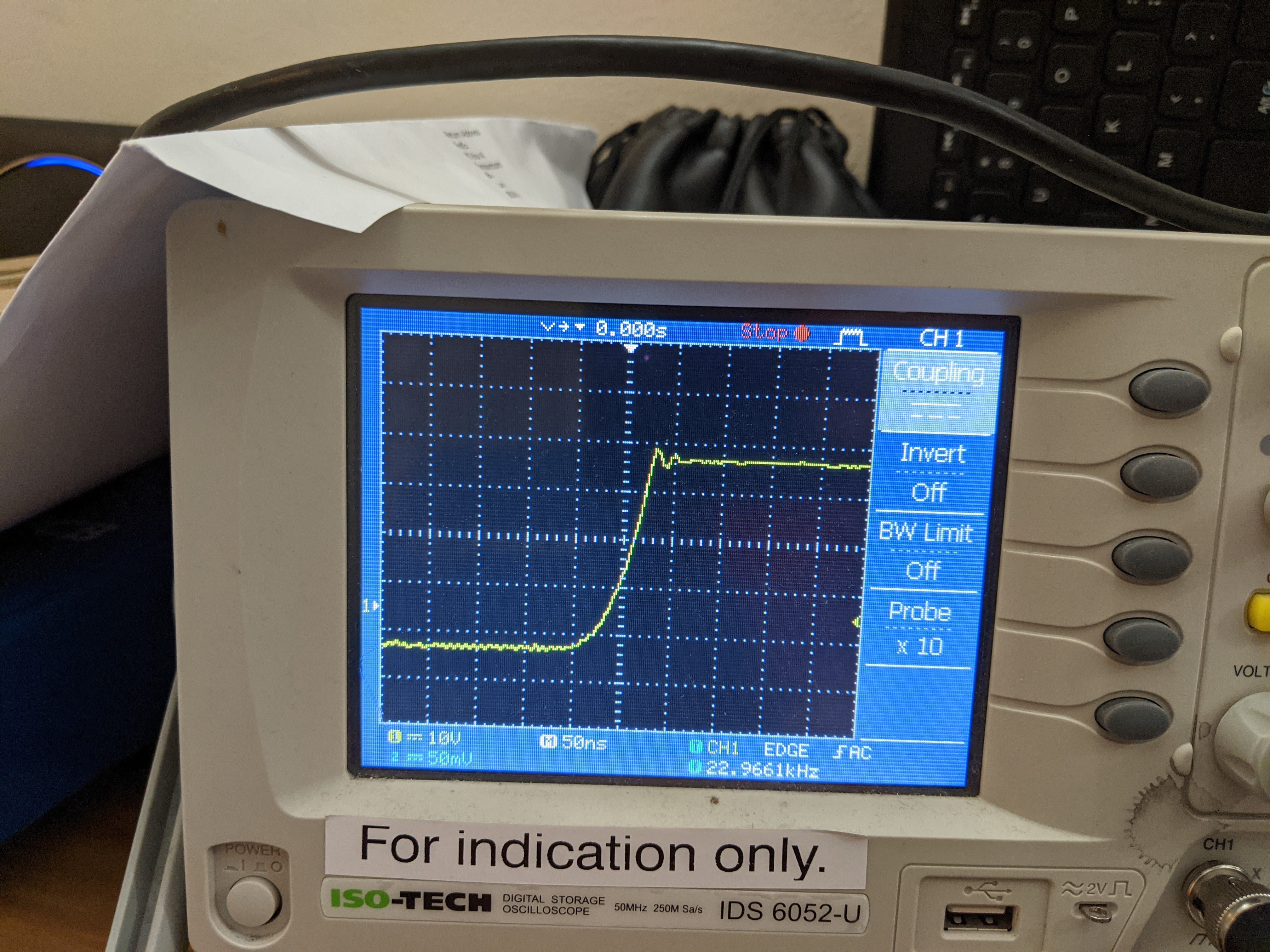
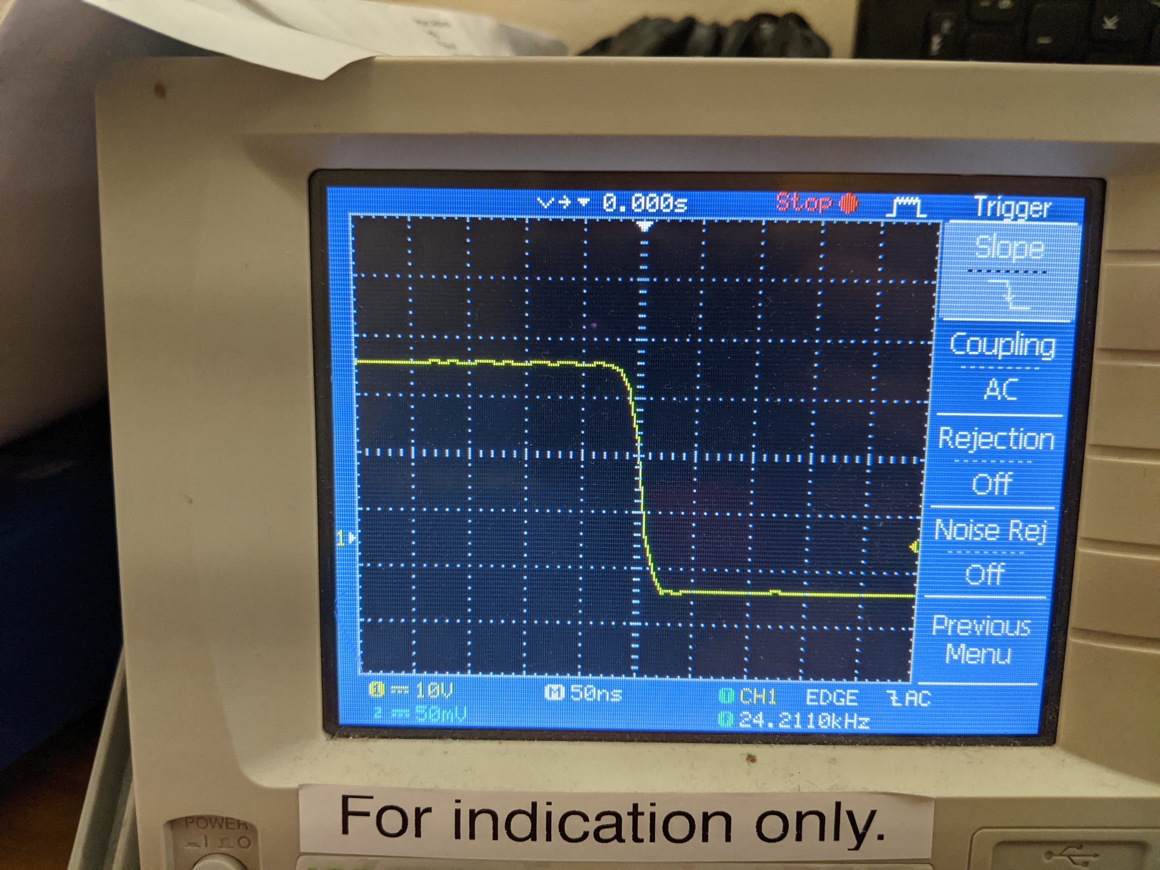
Current is only about 4A on my desk with the small motor. It's quite hard for me to get high currents at my desk with an EBike motor, they generate a load of torque, and when spinning have enough energy to grind holes in my desk.
A switching trace at 4A is worthless, you want to find how bad your voltage overshoot is, and V=L*di/dt. If your "i" is like 2% of your worst case scenario, then your measured overshoot is likely in the 2% range of what you will really have down the road.

That's why so much effort is spent getting the test rig right, a double pulse test doesn't need a high power supply, in fact you typically just charge the DC link and disconnect the power supply right before the test, especially when you want to make sure the short circuit protections can trip with the energy of the DC Link alone.

OK,

I am currently severely time and budget limited, so will not imminently have time to code or rewire for double pulse test, but I do have time for this:
MESC_FOC%20v0.5%2070A%20Id%205AIq%201.jpg

MESC_FOC%20v0.5%2070A%20Id%205AIq%202.jpg

MESC_FOC%20v0.5%2070A%20Id%205AIq%203.jpg

MESC_FOC%20v0.5%2070A%20Id%205AIq%204.jpg


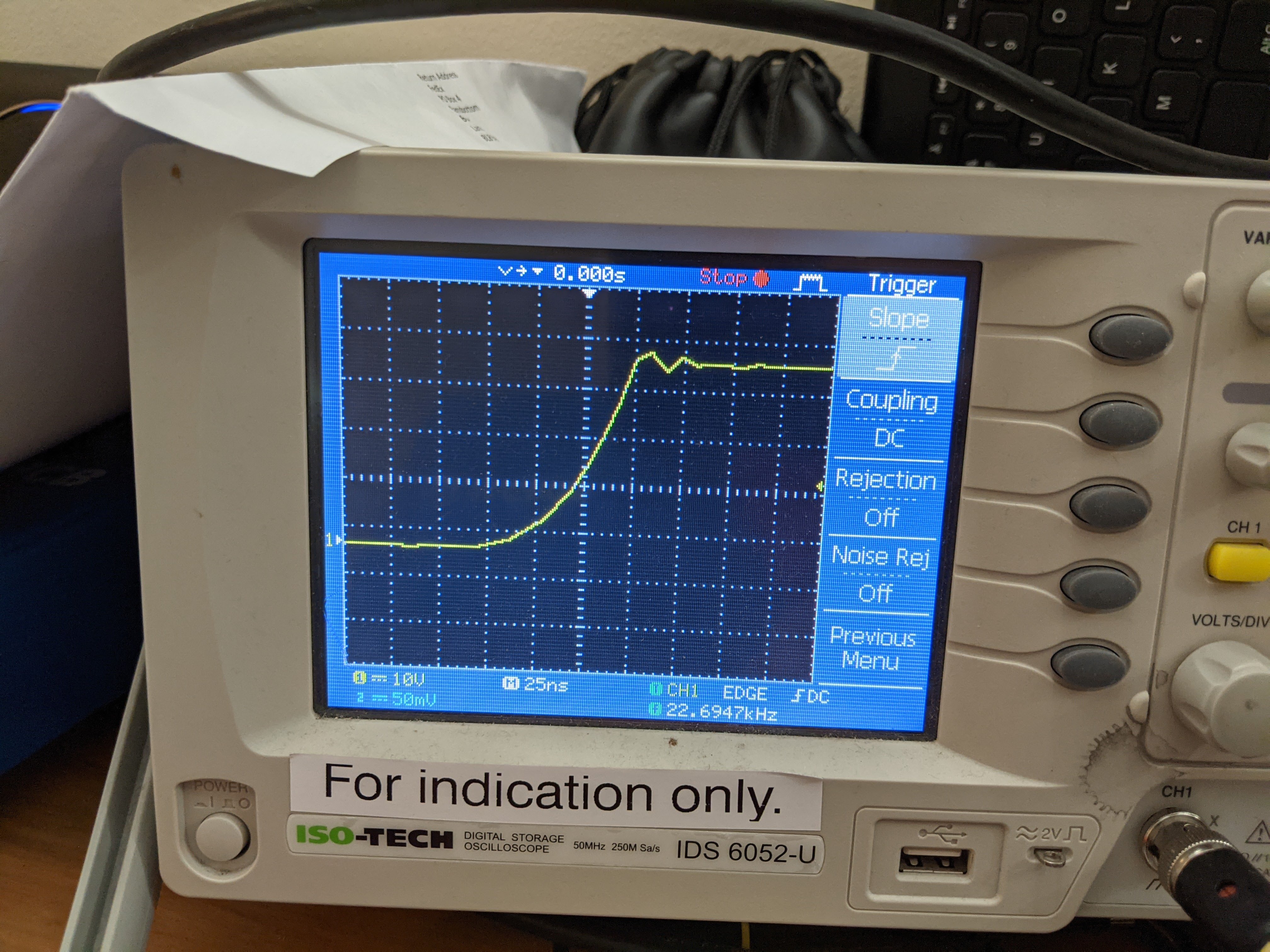
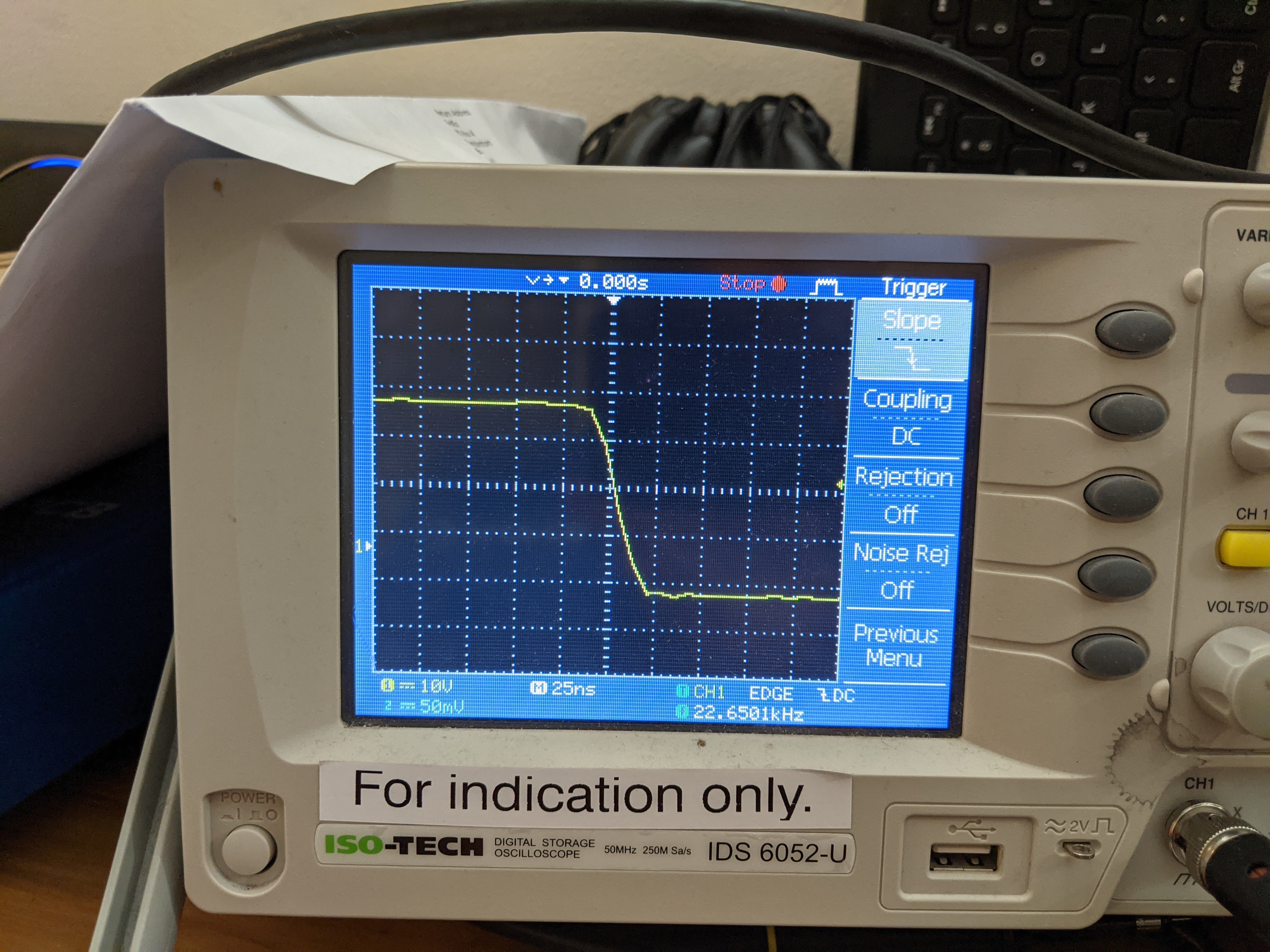
70A Id, 5A Iq, which corresponds to about 60A phase (IIRC, the conversion ratio from the Clark/park gives (sqrt6)/2).

At this power, the PSU is sinking >150W into the PCB/motor (the gauge fluctuates a lot around this value). The motor gets hot quite fast; over about a minute. The PCB gets... Warmish... FETs probably approaching 60 degrees with no heatsink after a minute or so. If I increase Id current any more, the PSU just starts to crap out. It's only got a 250W mains:DC rail, and I toasted my only Lithium battery...

Motor phase resistance is 40mohm, so sinking ~150W implies something in the region of 50-60A. Current traces on the shunts show current sin wave peaks are ~81A, so RMS current is ~58A.

Not really much more ringing or weirdness at this higher current. I really need a more expensive scope than this 250$ piece of junk from the early 2000s though. Looking longingly at a Keysight 200MHz 4 channel job... Think I might take the plunge after a few pay cheques.
 
Yes, don't trust too much a low end scope. This happened a few years ago, SiC powerstage.

Cheap 100MHz owon scope:
photo_2021-02-02_01-34-51.jpg

A Rhode&Schwarz scope:
photo_2021-02-02_01-34-47.jpg

Both probes were measuring exactly the same place in exactly the same way with those small gnd springs. Now our team has a couple of even higher end 1GHz R&S scopes for this kind of power electronics stuff, with these pics you can clearly see how big is the difference, especially when you are switching hard.
 
marcos said:
Both probes were measuring exactly the same place in exactly the same way with those small gnd springs. Now our team has a couple of even higher end 1GHz R&S scopes for this kind of power electronics stuff, with these pics you can clearly see how big is the difference, especially when you are switching hard.

Yes... Your team is doing this for money, I, me, a bored mechanical engineer, am doing this basically for shits and giggles in my spare evenings. Unfortunately this means I don't get to own many 1GHz Rhode and Schwartz scopes.

I'm thinking keyfit dsox1204g with 200MHz bandwidth upgrade. I can just about talk myself round to that level of expenditure. Reckon that will suffice? I see your ringing and nastiness in that pic is about 50MHz. Disappointing the 100MHz cheap scope barely resolves it.
 
This is long overdue, and I have been having all kinds of commentary on other threads, and one should show their own hand if professing to know sod all.

Double pulse test results below.

Tests performed using my 8080 70kV motor, with ~40uH phase inductance as the load.

The MCU was coded to turn on the PWM fully for 7 PWM periods (~30us/period), then a pulse at 10% duty for 1 PWM period, then freewheel and go into idle state. The modulation was done on phase W, with the current measured on phase V, which I observe to have the best current measurement (least noise)

The system was powered by fully charged 16s (4x4s) Turnigy Rapid packs 65V on the voltmeter, rated for 5.5Ah, 140C, and has 2x470uF electrolytics on the board in addition to the ceramic 1uF. I installed a 50A automotive slow blow fuse to protect myself from massive fires in the event of failure. I will not lie, I was slightly scared as I did this. The motor was making quite unpleasant thumping noises with each pulse. The wires are somewhat thin for this, and with 200A, some ~8% voltage drop can be seen. After pressing the "t" button on my keyboard (triggers the test via serial) a load of times, the wires were warm. But I don't really care about the wire's welfare, for my bench test rig where I am mainly messing with code, running 12awg gets quite irritating.

I did a series of tests building up the voltage before the final result posted below; 20VPSU, 16V single Turnigy, 12s 3xturnigy then 16s4xturnigy.

Current was measured using the output of the opamp, which has a gain of 16, with 2x1mohm=0.5mohm shunts. The final test's peak current is therefore of the order of 1.5V/16/0.0005ohm = 187A. The opamp is starting to saturate at this current, so the exactness of this is uncertain.
As a sanity check, with 40uH of inductance, 200us and ~60V, we would anticipate the current to be roughly V/L*dt=300A. Edit: 80uH for two phases so we would expect 150A, but with the observed saturation lowering inductance, it starts to ramp faster. Don't math at 1am in a rush. /Edit.

Considering resistances on the motor phase (~40mohm), opamp non-linearity etc... we can say the measured current is probably close to correct.
16s current.PNG
You can see the non linearity of the motor inductance in this, the current starts to rise much more rapidly above about 100A. You can see it start to saturate the opamp as it approaches 1.5V above resting current.
16s voltage zoomed out.PNG
Here we see the overall test, in voltage terms. The voltage sag in the system to resistances can be seen dropping the bus from 66V to around 61-62V.
16s voltage zoomed in.PNG
Here we see the two edges of interest
16s voltage falling edge.PNG
The falling edge at 187A. The undershoot is ~10V. I have my suspicions that this is partly due to the probe inductive pickup, since the changing current paths are smaller than the probe loop even with the ground spring... Maybe when it's not 1am I will retry with a twisted pair.
16s 187A voltage rising edge.PNG
The rising edge at 187A, again, 100MHz ringing, could well be probing causing a significant part of this...

Below we see the overall setup and the way it was probed. I have had to cut out some of the pic since I accidentally left some bank statements on the desk if anyone is wondering what's behind the white square...
Setup.png
Probing double pulse test.PNG

Conclusion: There is nothing atall unpleasant going on, even with the ultra fast switching, no snubbers etc. Considering I intended this board to be run up to ~100A, and I accidentally did this test at twice the current (I was thinking 1mohm resistors, forgetting there were 2 in paralell as I set it up...) I think this is satisfactory.

Maybe later I will try:
1) running 20s 100A
2) twisted pairs
3) more checking gates

But basically, dare I say it...

Ladies and gentlemen;
This is the way.
 
I had some awful experiences using off the shelf controllers and low kv motors, 50-80kv Alien Power Systems c80100s, trying to get them to start with VESCs required massive spikes of current. Something I'd not seen with higher kv motors, ~170kv.

Also those wires look awful thin to be slinging ~200A around! You'd want 12-8AWG at least!

Love the pictures
 
Update to the above, 40uH is phase inductances and I was going through 2 of these so 80uH before saturation observed. This looks closer still so I'm even more inclined to trust the opamp readings.

Yes the wires are way thin. I thought "I'll just code this up..."then tried it with psu... Then 4s.... Etc... And suddenly was at 16s 187A with the wires not scarily hot so thought sod it, run it as it is and get the pics.

I've had very little issue with the big motors from alien. In general I've found VESC to be not great for startup and general reliability. I have 2 VESC based controllers (flipsky and a custom...) they both suffer from juddering that feels like belt slip as they go through the hall: sensorless transition. I think there's something not right, not stable in the VESC code, but who's going to attempt to debug that...
 
Very nice, thanks for posting.
At 100MHz (assumed it's the freq. of the circuit, not a probe artifact) and with Coss=1.7nF (from the datasheet of IPT015N10N5 @60V) the inductance is 1.49nH, that is ~10% of the smallest achievable with TO-247, and the switching losses are much less.
Just a note that the undershoot on the FET is an overshoot on the other one, and normally higher. I know it is hard to measure the exact amplitude, but turning off 187A in 20ns on 1.49nH induces 14V, so don't be surprised if you see an overshoot in this magnitude.

The gate resistors are single 5 ohm?
 
Good insights. Managing the 14V undershoot, which limits the applicable voltage to 100V-14V so 86V, 20s could be useful. The question is how. Snubbers will probably suffer from a similar inductance, so will never be able to fix all but could well reduce it.

I doubt it's really possible to improve the inductance of the layout since the TOLL has an inductances of 1nH by itself according to the Infineon appnote. Perhaps swapping to the on semi equivalent fet that has larger output capacitance? Fdbl0200 or something like that.

This probably doesn't need managing tbh. 187A is a ridiculous amount of current for a board that costs <30$ to build. At 65V this is peaks of 12kW...

Gate resistors are single 4r7 0603. Driver is ncv5183 which has very strong drive capability. Very low output impedance.
 
Pinski1 said:
Also those wires look awful thin to be slinging ~200A around! You'd want 12-8AWG at least!

Wires are okay, I regularly do 700A tests on 2.5mm² wires. Pulses are so short that there is no time to damage them.


You might want to check your miller performance to see how badly Mr. Miller wants to turn ON your other mosfet.

Here is an example of miller that i have on the bench right now. Yellow trace is the gate, at 2.5V the mosfet would turn on :flame: :
image (23).png

That's after tuning. Before tuning it ringed and reached 4V. Wished a small gate driver with miller clamp.
 
The miller is one that has been making me hmmm and worry for a while. Mainly because I found
Parasitic bounce on gate 10x probe with switching of switch node.PNG
Parasitic bounce on gate 10x probe.PNG
on the gate.
The obvious candidate for this is miller capacitance, but I really do not think it is. The reasons are:
1) The time constant is different to the gate voltage decay as driven by the gate driver. Even if the voltage step is caused by Mr Miller, the decay back to equilibrium should be the same as the intentional gate pull down.
2) It comes and goes depending on the current magnitude and direction through the half bridge, even though the rise time remains essentially identical. If it was miller, you would probably not expect the current to make a difference.
3) I am able to make it exceed the gate turn on voltage without any evidence of shoot through/whatever by giving it 20s, which by Infineon's appnote https://www.infineon.com/dgdl/Parasitic_Turn-on_of_Power_MOSFET.pdf?fileId=db3a30431ed1d7b2011eee756cee5475 should be basically impossible for this FET.
4) There is no ringing induced by it (would be visible at low current, the ultra high current test induces enough artifacts to mask)

Practically, a 25ns pulse of miller nastiness is so incredibly short that it's probably not going to be a problem.

I actually started a thread on Infineon forums about this. I just realised they replied 2 weeks after I posted...
https://www.infineonforums.com/threads/12360-Parasitic-turn-on-in-IPT015N10

I think the cause of this spike is the output capacitance/reverse recovery charge getting dumped through the FET source incredibly fast as the switch node rises, which causes a small inductive kick. ST cover this in appnote https://www.st.com/resource/en/application_note/dm00061867-power-mosfet-technology-gate-current-needs-in-a-synchronous-buck-converter-stmicroelectronics.pdf
ST gate bounce appnote.PNG

This makes my situation for assessing this difficult - Infineon stating it is completely immune to turnon due to the Cgs:Cgd ratio and ST saying this is an inductive effect on the source bonding, while it clearly looks (almost) exactly like one would expect a miller turn-on to. The implication of it being due to package source inductance is that it is not a voltage experienced by the silicon/gate, and therefore won't result in parasitic turn on.

On balance, I am pretty sure this spike is inductive artifact, not miller. In which case, there is no evidence of miller, or it is small compared to the inductive bounce. I am convinced enough of this that until there is any evidence of it being a problem (heating, FET failures, Infineon retracting/providing an explanation for their appnote being bollox...) I do not intend to slow the switching to get rid of this artifact.

Of course, slowing the switching by reducing the low side gate resistor reduces the miller clamping ability. Adding a diode + 2 resistor arrangement increases the fall switching speed, and increases the problem on the top FET.

You then spiral into piling on complexity to fix a problem that probably doesn't even exist, with special gate drives and blah blah, and at the end you have lower efficiency due to switching losses, bigger heatsinks, a higher BoM cost, bigger boards, more things to go wrong... Everything I set out to avoid.

Yes, this is worrying me a bit, but I want to approach this via reasoned consideration of e.g. the output capacitance being dumped across 1nH, ideas for ways to make a truer Vgs measurement etc. I am not interested in approaching this from the "add more expensive parts to be sure" perspective; no one learns anything that way and I am not doing this for money.
 
mxlemming said:
Good insights. Managing the 14V undershoot, which limits the applicable voltage to 100V-14V so 86V, 20s could be useful. The question is how. Snubbers will probably suffer from a similar inductance, so will never be able to fix all but could well reduce it.

I doubt it's really possible to improve the inductance of the layout since the TOLL has an inductances of 1nH by itself according to the Infineon appnote. Perhaps swapping to the on semi equivalent fet that has larger output capacitance? Fdbl0200 or something like that.

This probably doesn't need managing tbh. 187A is a ridiculous amount of current for a board that costs <30$ to build. At 65V this is peaks of 12kW...

Gate resistors are single 4r7 0603. Driver is ncv5183 which has very strong drive capability. Very low output impedance.
I think it's very good as it is, at 100A the current turn off time would be less than 20ns with smaller overshoot.
RC snubber wouldn't reduce the overshoot, that is only useful to stop the HF oscillation.

For the miller turn-on it's hard to tell exactly what is going on on the internal Vgs because the Vds and the current on Ls change at the same time at the end of the reverse recovery.
 
Since the firmware fix, the current sinwaves have been improved substantially. PXL_20210311_231536175~2.jpg

This is 25A phase current trace from the opamp output. The switching scheme (sinusoidal/bottom clamp at high modulation) and low side shunts create all the odd oscilloscope artifacts, but the wave is clearly visible.
 
Of course, slowing the switching by reducing the low side gate resistor reduces the miller clamping ability

Another way to slow the switching is to add an external ceramic capacitor between the gate and source pins. It would also improve miller clamping without the need for pricy gate drivers with active miller clamps.

The generic Chinese boards get away with very simple transistor-based gate drivers by doing this. Haven't tried it yet but it'll be going in my next design.
 
thorlancaster328 said:
Of course, slowing the switching by reducing the low side gate resistor reduces the miller clamping ability

Another way to slow the switching is to add an external ceramic capacitor between the gate and source pins. It would also improve miller clamping without the need for pricy gate drivers with active miller clamps.

The generic Chinese boards get away with very simple transistor-based gate drivers by doing this. Haven't tried it yet but it'll be going in my next design.
In my ongoing quest for lower gate capacitance, I'd never even considered adding more gate capacitance. You're right though, it probably is the better option than slowing down the switching with higher resistance, since it both decreases the miller effect and slows down the transition giving the resistor/driver more time to pull down the gate...
This will be my solution if it turns out the miller IS a problem.

I have a plan. I'm going to artificially bump the switch node voltage with the low side gate unattached, but switch and gate pulled to 0V just prior to the experiment. I should then see the miller capacitance bounce the gate without decaying into the gate driver, so it will be visible after all transients are over. The only decay will be due to scope and gate leakage. If necessary i can buffer the gate with an opamp (got some lmc6484 kicking about from years ago... 20fA leakage current).

This will verify the input to Miller capacitance ratio, and if i do it at a few voltage levels I'll be able to replicate the miller capacitance vs voltage curve. Any excess over this jump when used in double pulse/motoring is therefore inductive/artifact.

Hopefully we can then close this down for good with a complete understanding.
 
External Cgs is a very strong tool against miller. I use it most of the time, and always place the footprint.

Just keep in mind the extra avg current on the gate driver and that the cap tolerance is really bad compared to the typ 1% resistor.
 
Marcos can you tell a few things about the circuit that produced the waveform you attached above, if these are not secrets?
FETs, Rg_on, Rg_off, if external Cgs is used, current sensor is under the low side FET or on the phase output, and the current at this test?
 
peters said:
Marcos can you tell a few things about the circuit that produced the waveform you attached above, if these are not secrets?
FETs, Rg_on, Rg_off, if external Cgs is used, current sensor is under the low side FET or on the phase output, and the current at this test?

This does not look like a double pulse test to me. Certainly not a 700A test as alluded to (Marcos never actually says that waveform is from a 700A test). With rise and fall times similar to mine, much faster than yours, and assuming the same physics you've described to explain the overshoot, it would take some kind of voodoo to get the waveforms pictured with 700A current, not just twiddling gate resistors and capacitors.

Or maybe it is all scope artifacts we're seeing and his R&S beast just works better :lol:
 
No, I didn't think it's a 700A test. :)
If I can guess it's with SMD FETs at relatively low current intended specifically to test the Miller turn-on. Inductance is low because there are no signs of inductive voltages, but there is some current because of the fast 30V jump at the Vds rising edge that indicates the end of reverse recovery. I reckon there is a higher Ron and a lower Roff with a reverse diode, because of the shape of the decays of the negative and positive bumps, and without Cgs. The 1.46V Vgs rise for the 30V Vds jump suggests 1:20 ratio for Crss vs. Ciss that can be normal, because Crss is high at lower voltages, but I'm wondering which FET it is and if the graph in the datasheet matches that.
 
marcos said:
External Cgs is a very strong tool against miller. I use it most of the time, and always place the footprint.

Just keep in mind the extra avg current on the gate driver and that the cap tolerance is really bad compared to the typ 1% resistor.

I also agree adding some Cgs can work wonders, but it can really stress a gate drive that isn't up to the task. I recently built a boost 30A SMPS that runs at 400kHz and had 3.3nF added G-S, the IC ran at about 80C. With the 3.3nF removed (it wasn't needed) the IC ran at 60C. I decided I'm quadrupling the inductance and going to run at ~100kHz because the driver isn't very strong.

Here is a scope shot of +100A on a big DC link layout which had about 65nH and many parallel devices. Total current was just over 1kA on the bus. I also ran big negative bias with a clamp, so miller turn on wasn't really an issue, but the G-S cap quelled a lot of noise and overshoot, just needed a beefy gate driver.
G-SCap.png
 
peters said:
Marcos can you tell a few things about the circuit that produced the waveform you attach

That one was at 100Amps I think. At 200A I start to see some artifacts despite the large Cgs=10nF

Can't share the mosfet # or topology, but the typical doc package looks like this
image (24).png

And tests with RgOFF:1.5ohm and RgOFF 3.3ohm at 200A.
image (25).png

PS: I won't pretend to know why the waveforms look like that, I just learned to tune knobs and make fancy PCBs, still far from the die-level insight that Peters and Zombiess have
 
marcos said:
peters said:
Marcos can you tell a few things about the circuit that produced the waveform you attach

That one was at 100Amps I think. At 200A I start to see some artifacts despite the large Cgs=10nF

Can't share the mosfet # or topology, but the typical doc package looks like this

Marcos, could you share a pic of the probing technique you're using to get these waveforms? What probe, connection, extra impedances etc. Cover up the part numbers, draw a picture or something.

At the moment, my inclination is that a lot of what I'm seeing is residual probing and scope artifact, since Marcos' mega scope shows none of this, and with similar rise/fall times and it being virtually impossible that he has lower inductance on his board, I can't really see how one could make a step change like this. This isn't SiC/GaN with ultra special packages is it Marcos? If so, your switch speed, reverse recovery etc could be far faster and all bets are off when the rest of us are playing with silicon.

At 100mhz ringing, I'm on the limit of my scopes stated ability, and with the 65V swing and 200A, it would be very easy to be picking up all kinds of common mode interference, scope amps hitting internal dv/dt limits, inductive coupling on the tiny grounds loop...

So I'm wondering what improved techniques to use...
Twisted pair straight to the ground and switch node?
Divide down the switch node to a range more friendly to the scope e.g 10k and 100k ground to switch node?

Peters, your calculation for the overshoot of 14V i presume comes from V=Ldi/dt =1.5nHx187/20ns? This doesn't account for the output capacitance of ~4nF which with i=C dv/dt gives dV= (187/2)/4nx20n=465V which is a significant though not majority effect compared to the voltage swing if 65V. There's also the diode reverse recovery charge of 213nCx2 which over 20ns would result in a 20A reduction in the di/dt component. Then there's(small) PCB capacitance... All of these reduce the effect of Ldi/dt. Any chance with all these accounted for the overshoot could be basically zero like Marcos measures?

Sometimes I like to flip the problem on it's head. Say I really wanted to get great ringing, as much as possible, I ask "what would stand in my way of getting great ringing".
 
Thanks, very informative waveforms, good to know that such low inductance is feasible.
But I think I would try to switch this circuit faster to reduce the switching losses, at least the turn-off, even if that would induce higher overshoot. But it's my personal preference. The Vgs and Vds rise and fall times are similar to mine with TO-247, the big difference is obviously my slower current transitions due to the much higher inductance. To my mind the artifacts are normal up to some level if they are reasonable and do not exceed the max. ratings.

I'm a bit more cautious with the added Cgs that clamps the external Vgs, because of Ls*di/dt. If the artifacts induced by di/dt are cleaned from the external Vgs with the capacitor, then these artifacts may be moved on the chip inside the case with reversed polarity and remain hidden. But it is more for TH packages with high Ls.
 
mxlemming said:
So I'm wondering what improved techniques to use...
Twisted pair straight to the ground and switch node?
Divide down the switch node to a range more friendly to the scope e.g 10k and 100k ground to switch node?
Maybe a short twisted pair or shielded wire soldered or contacted to the pins with the smallest loop. Try a wire loop similar to the one I used to pick up di/dt, but smaller, with that you could find the probe orientations where there is no induced voltage.
Resistor divider would just reduce the bandwidth, unless it is frequency-compensated with parallel capacitors.

Peters, your calculation for the overshoot of 14V i presume comes from V=Ldi/dt =1.5nHx187/20ns?
Yes, and V=Ldi/dt is always true for the inductance.

This doesn't account for the output capacitance of ~4nF which with i=C dv/dt gives dV= (187/2)/4nx20n=465V which is a significant though not majority effect compared to the voltage swing if 65V. There's also the diode reverse recovery charge of 213nCx2 which over 20ns would result in a 20A reduction in the di/dt component. Then there's(small) PCB capacitance... All of these reduce the effect of Ldi/dt. Any chance with all these accounted for the overshoot could be basically zero like Marcos measures?
With an ideal (very fast) switch the equation for the energy transfer would be valid: 1/2L*i^2 = 1/2C*V^2. With L=1.5nH, i=187A and C=4nF -> V=114V, that would be the overshoot over the DCbus voltage.
But the real switch (FET) has some turn-off time, so a part of the energy from the inductor is dissipated on the switch while turning off, and only the residue charges the capacitor.
Also in practice the turn-off time is slower than the half of the period of the natural frequency of the LC circuit, so the di/dt and the overshoot is limited by the switch, not by the LC circuit.

The diode reverse recovery applies for the turn-on only, not for the turn-off overshoot. That is when the diode of the other FET changes from forward conduction to reverse voltage.

There is overshoot also in Marcos's waveform (5..6V?), and also notice that the timebase is 500ns/div while yours is more zoomed in. The cut-off corner at the start of the Vds falling edge also indicates the inductance, that must be really very low, maybe half of yours?

There are some options if you want to experiment: maybe remove the current sense resistors from the loop and put them on the phase output and move the part closer, put the 2 FETs and the ceramic capacitors in a row and return the current underneath on the next layer (the loop would be squeezed between 2 adjacent layers instead of the planar loop on the surface), DirectFET, IMS board... but I don't know if any of these would be better.
 
For Marcos to have 1/2 the inductance, he must have smaller packages since most of my inductance is from the TOLL source. Direct FET or maybe even high power dfn8s or something. In turn this likely means the max power limit due to to heat is likely lower, or a lot more packages. Probably into the world of trade offs...

Changing to phase shunts would help reduce, maybe up to 1/3 but that's got big implications for the cost etc. Next board I make perhaps.

Thought about routing on inner layers. Could definitely reduce inductances. However, big problem is the inner layers tend to be thin and have little cooling (fr4 is very insulating). You can't reinforce them so you'd have to come up with an arrangement where it's routed on the outside as well, or the board is going to burn.

IMS is simply outside my price range for this.

We're thoroughly into the academic pursuit here. My board works far better than I'd ever intended it to from a switching perspective, it's probably time for me to accept it as is and start focusing on the sensorless startup, sensorless observer and a bit of safety (watchdog) plus better ui.
 
From the pics I think my board has at least 1/2 the parasitic inductance and stiffer dc link.

The low side shunt, wire bonding inside your fet, the caps arrangement, the stackup, they are all increasing your parasitic inductance. In my board miller is limiting both turn on and turn off swiching speed. In any case, looked acceptable so its running on the dyno now.

If it were GaN you would see 5ns rise/fall times, if it were SiC you would see a negative gate bias for the turn off, the ones I used had a super low Vgs(th) so miller clamp wasnt enough. With alum you try to keep layer count low to keep good heat transfer, so the waveforms don't look so nice.

I can't show this board but the measurements were just using the original scope probes, always using the gnd spring. Maybe induced noise is low because all current loops are very tight (low EMI). Havent done pre-compliance testing on this one yet, hopefully I will someday.
 
Back
Top