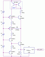
even simpler/cheaper LVC :)

curious

1 kW
Joined
Dec 29, 2007
Messages
445
Location
NJ, USA
I've been toying around with current-mode chaining of LVC circuits in the simulator recently and realized that you can build a super-cheap LVC using just one TC54 chip and current mode transistor chain as a sensor/aggregator. It will not have the same threshold accuracy and temperature stability as multiple TC54 circuit but it is not really needed for LVC-only circuit. The circuit allows building sub $1 LVC-only device (excluding board cost).

Few notes:
1. R1 has a smaller value because top segment of the chain connects directly to the cell, not to the collector of another transistor above (which can have higher potential than corresponding cell by Vbe-Vce_sat). By properly selecting R1 threshold of the top cell can be made equal to other cells (even though measurement slope will be slightly different).
2. Q4 buffers very high-Z output of the measurement chain.
3. D1 can be replaced with another transistor in a diode arrangement.
4. With some rearrangement the circuit can be thermally compensated. I did not do it here for readability/simplicity reasons and also not convinced it is needed in real life.
5. A high impedance voltmeter attached to the anode of D1 or emitter of Q4 gives you approximate readout of the lowest voltage cell (with proper resistor choice and scaling).
 
Without sticking that in a simulator, I coudln't say for sure, cuz I sometimes have trouble picturing things right, but arent' there likely to be points where the voltage across one of those 3906 transistors is going to be awfully high? Beyond their max Vce? (assuming typical ebike sized packs)

ALso, I'm not quite sure that I get how it would work--wouldn't it require all the cells below a particular cell in a chain to be low before it would read the next one up?

I'm probably just not getting it due to oldtimers', but an explanation of the stages of circuit operation would be helpful to those non-engineers among us. ;)
 
amberwolf said:
...voltage across one of those 3906 transistors is going to be awfully high?
No, it is split more or less evenly, not exceeding single cell voltage, certainly not full pack voltage.

amberwolf said:
...an explanation of the stages of circuit operation would be helpful to those non-engineers among us
The top segment sources current proportional to the cell voltage which is propagated along the chain. This current causes equal voltage drop across resistors at each stage. If any stage sees cell voltage below the voltage dropped by its resistor, the transistor at the top of that stage saturates, sinks all current coming from the top of the chain into the base and disconnects the chain. Hence the lowest voltage cell becomes the current source of the entire chain. The lowest cell wins "arbitrage". Again that current is proportional to the voltage of the lowest cell hence the lowest cell voltage can be read out at the bottom segment resistor.

On a different note, regarding temperature compensation. If D1 is replaced with another 2n3906 the circuit has very good temperature stability, except for the top cell. I ran temp sweep in the sim from 20 to 100C and the voltage at tc54 input varies by about 2% (with a single cell set low intentionally). This is expected as Vbe(t) of the bottom transistor is compensated by Vbe(t)-Vce_sat(t) of the top transistor at each stage and the final buffer is compensated by the diode (or transistor). The top segment temperature stability is notably worse again as expected. Even though it is not big deal for LVC, perhaps for perfection only reasons I will do the top segment differently.
 
So whats the average current draw of the circuit? Will it drain the pack if left connected?

Cheers, Adrian
 
adrian_sm said:
So whats the average current draw of the circuit? Will it drain the pack if left connected?
About 4uA, good for few decades, perhaps more...
 
Warning, the following post is for perfectionsists and analog circuitry fans only :)

Here is the temperature compensated version with the ideal/regular top segment (not practical as it requires extra power supply for current source I1). It is quite accurate and can be used for analog measurements of lowest cell V at the output:
View attachment 1

The top can be folded using a current mirror and measurement for the top segment done in the right side mirror path. Now I1 is perfectly doable although the solution obviously doubles the circuit current consumption:

Again this circuit is accurate enough for analog measurements of lowest cell V.
 
I'm going on a hint of an idea that I overheard from someone at a pub a long time ago...(forewarning that I don't know shit about circuits) ... but aren't transistors sensitive to small temperature changes? If this was attached to a cell that was on the warm side, is it possible it might cut off earlier than it should?

EDIT: I see you have already covered this. Nevermind, carry on :)

I think the principle you have is one of three functions that the likes of EV-Power BMS modules use. But yours would be markedly cheaper!
 
just a small note but dosnt the .7-.9v drop across the transistor get multiplied by the number of transistors in line from the low cell ... and wont their be a drop across the diode aswell ..
or am i just seeing it wrong(could be)
i am in many ways like a cave man poking fire w/ a stick trying to get it as far as circuits are concerned but if i am wrong plz correct me and let me know were i am not seeing it wright so i may learn from this and become stronger
 
oh and i forgot to ask ... what program are you using to sim/draw the circuit
 
nebriancent said:
oh and i forgot to ask ... what program are you using to sim/draw the circuit
LTSpice. It is a nice completely free SPICE simulator with graphical front end supported by Linear Technology.
 
I have finally built and tested this LVC-lite circuit for a 16s A123 pack. The pictures from this thread were lost so here is another one:
lvc_lite.GIF
As I said before it is not as precise as multi-TC54xx chain but for a123 lifepo4 cells the LVC detection accuracy is quite adequate. The circuit is temperature-compensated.

The downside of the circuit is that it underestimates the cell voltage by about 0.2V (transistor Vce saturation voltage) at the test point A *if* multiple cells have voltage close to the smallest voltage cell (whatever that value is). OTOH if there is a single cell in a pack that is 0.2V lower then others the circuit reports fairly accurate analog voltage value of the lowest cell at the test point A. I can live with this limitation. Test point A is connected to the TC54xx comparator and can be also wired to a high impedance voltage meter.

For a prototype I used a mix of through hole transistors and SMT 0805 resistors. The circuit lends itself to a nice regular layout, such that using a plain 0.1" grid prototype board it is possible to build it with very few extra wires. BCV62C is a SMT current mirror. Measurement 1M resistors R1..RN are 1%.
 
Cool.

I'll have to think about that a bit. I don't fully understand how it works at first glance.

It looks like maybe the current in the series chain is a function of each cell's voltage. The cell with the lowest voltage controls the current in the chain. The chain current is sensed by the TC54 and can trigger at the desired set point. Does that sound about right?

I've always like the cascaded chain approach as it eliminates optocouplers. One thing I'm not sure about is how well those microamp paths will behave in the presence of PWM switching noise. Some filtering may be needed, but the TC54 has some filtering built in.
 
fechter said:
It looks like maybe the current in the series chain is a function of each cell's voltage. The cell with the lowest voltage controls the current in the chain. The chain current is sensed by the TC54 and can trigger at the desired set point. Does that sound about right?
That is exactly how it works, except the top cell which needs to be mirrored (there is no voltage "above" the top cell to make it exactly the same). It gets a bit tricky when the transistor goes below Vce saturation (typically around 0.15-0.25V) and the gain starts dropping which leads to chain current loss - hence the 0.2V inaccuracy.

fechter said:
I've always like the cascaded chain approach as it eliminates optocouplers. One thing I'm not sure about is how well those microamp paths will behave in the presence of PWM switching noise.
It was a logical continuation of your chained circuit. The other, more precise (but more expensive) version with individual TC54s may look like this:


fechter said:
Some filtering may be needed, but the TC54 has some filtering built in.
Perhaps (I have not yet tried this LVC on a bike). But the current is so low that parasitic capacitance of chain elements and TC54 input plus 0.1V hysteresis of TC54 may be enough. Anyway shunting TC54 input with a 10-100nF ceramic cap costs virtually nothing and probably should be done.
 
Yes, when breadboarding the chain circuit, I found I could trigger it just by touching a wire. Adding a capacitor will definitely help and there is no reason the circuit needs to respond super fast.

What's really cool about this configuration is you could adjust the trip point on all the cells with a single adjustment.
 
Thanks for posting this idea. Any plans to alter it for HVC too?
 
That might be more difficult, as the current in the chain will be limited by the lowest cell.

There might be a way. Have to digest that thought for a while.
 
IBScootn said:
Any plans to alter it for HVC too?
You mean transistor only or transistor/comparator version ? Transistor-only chain will not be accurate enough for HVC/balancer application (even if it can be designed). Comparator-transistor chain can be modified fairly easily for HVC/balancer apps. I think fechter and Gary already have few versions of it (although most of the pictures were lost during website transition, can't check what they did).

You can even re-use the same signaling chain to save parts if you do not plan to use HVC/LVC simultaneously. But I kind of like to keep LVC and HVC/balancer circuits separate. My LVC circuit has a piezo beeper and it is permanently attached to the battery pack, not to the bike. This way even if the battery is in storage it can still tell the entire house that it is unhappy :)

OTOH HVC/balancer (resistor type) belongs to the charger in my view. Resistor balancers dissipate quite a bit of power and cooling fan in the charger helps a lot. If it is a microprocessor charger the balancer integrates well with the cell voltage sampling and allows to start balancing well before the end of the charge saving quite a bit of time.
 
curious said:
You can even re-use the same signaling chain to save parts if you do not plan to use HVC/LVC simultaneously.

Really - that is exactly what I want. I only use HVC while charging and only use LVC while riding. Brilliant!
 
IBScootn said:
Really - that is exactly what I want. I only use HVC while charging and only use LVC while riding.
I assume you are going DIY route. What chip do you want to use to detect the HVC threshold ? Is it HVC only or HVC/balancer ? I can probably help you interface the chip output to the signaling chain.
 
What about to use these cheap balance modules for HVC?
http://www.ev-power.eu/SBM-CBM-1-1/Cell-Ballancing-Module-3-60V-1-7A.html

I added signaling LEDs on mines and with a simple additional circuit and your LVC we have complete BMS balancer.
 
Back
Top