Power stage for Brushless controller

nieles

10 kW
Joined
Jul 14, 2008
Messages
683
Location
The Netherlands
hey guys,

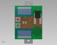
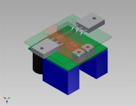
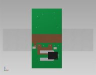
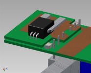
so i had this idea in my head for some time now, and decided to make a 3D mock-up
this is a single phase, so three of these will form the power stage for a controller

caps:
2x 4,7uF poly caps (max ripple current 9A rms, 5,3mR ESR)
2x 330uF el. caps (kze type)
2x 1812 ceramic cap

power terminals:
M4 thread (datasheet)

current sensor:
ACS758

Mosfets:
TO-247

what do you guys think?
I would like to hear your comments/criticism!
Also, check out the 3D PDF

dimentions what you see in the pictures: 50x75x45mm (LxWxH)
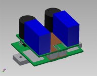
controller1 (1).jpg

the grey area on the bottom pcb is where the MOSFET driver will be.
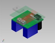
controller2 (1).jpg
View attachment 3
controller4 (1).jpg
controller5 (1).jpg
(3D PDF)
 
What is the part number on the 4.7uF cap that does 9a rms? Seems like a very mall value.

I have played around with sandwich designs similar to that, but only with the gate driver on the other board. My new powerstage layout is 4 layers because it is important to keep the DC buss overlapping to reduce radiation which stray inductance loves to pick up.

What about expanding it out to 2 parallel fets?
 
part number for the poly cap is B32674D3475. here is the datasheet
it is 11A rms actually. i remembered the value from the 3.3uF i had picked first.

yes you are right, the layout is still not optimal. not sure if switching to a 4 layer board would help in this case, gets hard to picture it in your head with 4 layers lol.

i have been going back and forth with the single fet and 2-3 fets parallel, i think i want a 6 fet controller running reliable first (which i have an application for)
then do a similar design with more fets in parallel.

my biggest problem is probably that i am trying to make it as compact as possible. i should just make one and get it running reliable then focus on possibly making it more compact.

are you ready to share your pcb design? i would love to see it, and maybe steal an idea or two:p

what do you think about the power terminals? i am very keen to give those a try. 3 buck a piece
i only worry they will not work, with the board warping when beefing up the traces
 
Ii can't see if they "have to" in your design, but the fets look like they could be closer, and you could align the output for even smaller parasitic, like this:

i.png
 
okay after thinking about it for a while, i think the dual board layout isn't going to work very well. (boards warping etc.)

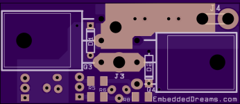
so what about this layout?

Top side will be Vbat+ and Bottom side will be GND.

controller2-1 (1).jpg
controller2-2 (1).jpg
controller2-3 (1).jpg
 
Having the power planes overlap each other is good design. Try to avoid having your gate input overlapping part of the power pass, looks like it might overlap part of the phase output, but it's hard for me to tell. If it does overlap, make sure the traces run at 90 degrees to it. I just had this conversation with HighHopes who was evaluating one of my parallel layouts. It took a lot of revisions and thinking but I think I figured out how to do parallel setups while still meeting strict design criteria. It's incredibly hard to come up with a good parallel layout. On my first TO-220 design which is soon going to the proving stage by getting put on my bike my gate input crosses the phase output so I violate the power pass rule, but so far so good in bench testing. The higher in power you get the more critical this becomes. Only road testing will tell me if I'm OK or not in my 4 parallel TO-220 design.

On my new design which uses 3 parallel TO-247 MOSFETs I decided to go with a 4 layer board as it was the only way I could keep fully over lapped power busses. I have high current on the top which will be built up with copper bar, then the other side of the buss is on 1 of 2 an internal layers since it's low current. The phase output is on the bottom layer. It's a similar configuration to a Xie Chang EB224/ EB236 controller, but with much better design. Snubber caps are VERY close to the pins and I could technically attach them directly, but I want everything mounted on the board for easy assembly vs adding them on later as I have done in the past when modding the Xie Changs.

The design will be posted and is open for anyone to use. It designed in KiCad and I'll be posting the Gerber files as well. I'm so close to finishing it, but I need to finalize how I'm attaching my gate drivers to them. I'll post up the entire design in a new thread for discussion on here.

Starting off with a 6 FET controller makes design soooo much easier. Paralleling is a PITA. It's the hardest puzzle I've ever tried to solve since not only do you need to think/design in 3d, you also have to picture what the magnetic flux lines are going to look like and there are many strict layout rules as I found out. Not easy! But it is fun :)
 
zombiess said:
Try to avoid having your gate input overlapping part of the power pass, looks like it might overlap part of the phase output, but it's hard for me to tell.

you are right, part of the gate driver circuit will overlap on the phase with this design

zombiess said:
It's incredibly hard to come up with a good parallel layout.

i came to the same conclusion :( that is why i am doing a single fet controller first (also i don't have an application for a high power controller)

i keep coming back to a dual board setup
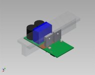
this is what i have in mind now:
controller2-5 (1).jpg
this is basically a 4 layer setup minus the cost of going 4-layer.
the back of the small pcb could be a EMI shield for the Gate driver on the main pcb (with its own gnd planes)

zombiess said:
The design will be posted and is open for anyone to use. It designed in KiCad and I'll be posting the Gerber files as well. I'm so close to finishing it, but I need to finalize how I'm attaching my gate drivers to them. I'll post up the entire design in a new thread for discussion on here.

Nice!looking forward to see your design. i only need a 1-3kw controller controller right now, so a single fet setup should be sufficient for me
 
I keep coming back to 2 board setups as well. Latest is a 4 layer for the MOSFETs, then individual 2 layer boards for the drivers. Part of the reason for this is my constrained packaging requirements. Layouts take many hours, many of which I just stare at the screen and figure out how not to violate the rules.
 
Back
Top