www.cellwise- semi.com CW1274-DS V1.4
0 2019-2020 Cellwise Microelectronics 1
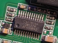
CW1274
4 ~ 7 battery protection IC
Functional characteristics
The charging protection
• The threshold range is 3.650V, 3.850V, 4.175V ~ 4.350V,
25mv step, ± 25mv accuracy
The discharge protection
• The threshold range is 2.300V ~ 2.800V, 100MV steps,
± 30mv accuracy
Disting overcurrent protection
• Overcurrent detection 1
The threshold range is 0.050V ~ 0.100V, ± 5mv accuracy
• Overclocking detection 2
The threshold range is 0.100V ~ 0.200 V ,, ± 10mv accuracy
• Short circuit protection
The threshold range is 0.200V ~ 0.500V, ± 20mV accuracy
Charging overcurrent protection
• Threshold range -0.010V ~ -0.050V, ± 5mv accuracy
temperature detection function
Construction and discharging high and low temperature protection, the temperature can be set on the outside
Balanced function
Broken wire detection function
Load detection function
能 function
Low -power design
• Work status 20 2A (25 ° C)
• Dormation status 5 2A (25 ° C)
S Packaging form: ssop24
Application field
vacuum cleaner
Electric tools
Electric bicycle
The backup power supply
锂 Lithium ions and lithium polymer battery packs
Basic description
The CW1274 series products are a highly integrated 4 ~ 7 string of lithium ions
Battery or lithium polymer battery protection chip. CW1274 is a battery package
Provide over -charging, overloading, charging and discharge overcurrent, disconnection, charging and discharge over temperature
Protection and equilibrium functions and support chip -level use.
CW1274
2 © 2019-2020 Cellwise Microelectronics
Typical application box diagram
CW1274
1 0
1 1
12
VC0
VSS
CS
7
8
9
VC3
VC2
VC1
4
5
6
VC6
VC5
VC4
1
2
3
VDD
N C
VC7 2 2
twenty three
twenty four
CCHG
CTLC
CTLD
19
2 0
twenty one
RCOT
RDOT
Cit
1 6
17
1 8
Sel0
SEL1
Rut
1 3
1 4
1 5
D O
C o
VM
Pack+
Packbattery Pack
CW1274
0 2019-2020 Cellwise Microelectronics 3
Product selection guide
Cw1274 x x x x
Form of packaging, s: s: ssop24
Parameter type, from A to Z
Battery type, L: represents lithium ion battery F: representing iron phosphate battery
Function and version information, from A to Z
product list
Product number
Overcoming threshold
[VOC]
Delay
[TOC]
Overcoming
[VOCR]
Trend threshold
[VOD]
Delay
[TOD]
Discharge
[VODR]
Balanced turn on voltage
[VBAL]
CW1274ALAS 4.200V 1S 4.100V 2.800V 1S 3.000V 4.075V
CW1274ALBS 4.250V 1S 4.150V 2.800V 1S 3.000V 4.125V
CW1274ALCS 4.250V 1S 4.150V 2.500V 1S 2.800V 4.125V
CW1274ALDS 4.250V 1S 4.150V 2.500V 1S 2.800V 4.125V
CW1274ALFS 4.175V 1S 4.075V 2.700V 1S 3.000V 4.050V
CW1274ALHS 4.175V 1S 4.075V 2.700V 1S 3.000V \
CW1274ALJS 4.250V 1S 4.150V 2.700V 1S 3.000V 4.125V
CW1274ALKS 4.200V 1S 4.100V 2.500V 1S 3.000V 4.075V
CW1274ALLS 4.250V 1S 4.150V 2.700V 1S 3.000V 4.125V
CW1274AFAS 3.650V 1S 3.550V 2.300V 1S 2.700V 3.525V
Product number
Overcurrent 1 threshold
[VEC1]
Overcurrent 2 threshold
[VEC2]
Short circuit threshold
[Vshr]
Charging overcurrent threshold
[VCOC]
Charging overcurrent delay
[TCOC]
Low -voltage prohibit charging
CW1274ALAS 0.050V 0.100V 0.200V -0.020V 0.5s does not support
CW1274ALBS 0.050V 0.100V 0.200V -0.020V 0.5s does not support
CW1274ALCS 0.050V 0.100V 0.200V -0.020V 0.5S 1V
CW1274ALDS 0.100V 0.200V 0.400V -0.020V 0.5S 1V
CW1274ALFS 0.050V 0.100V 0.200V -0.020V 0.5S 1V
CW1274ALHS 0.050V 0.100V 0.200V -0.010V 0.5S 1V
CW1274ALJS 0.050V 0.100V 0.200V \ \ 1V
CW1274ALKS 0.050V 0.100V 0.200V -0.020V 0.5S 1V
CW1274ALLS 0.050V 0.100V 0.200V -0.020V 0.5S 1V
CW1274AFAS 0.050V 0.100V 0.200V -0.020V 0.5s does not support
CW1274
4 © 2019-2020 Cellwise Microelectronics
Pinching diagram
CW1274
1
2
3
4
5
6
7
8
16
15
14
12 13
11
10
9
VC4
VC3
VC2
VC1
RCOT
Cit
Rut
VDD
CO
VM
DO
VSS
CS
RDOT
VC0
SEL1
20
19
18
17
twenty four
twenty three
twenty two
twenty one
VC7
VC6
VC5
Sel0
CTLC
CTLD
NC
CCHG
Number name pin description
1 VDD chip power supply, connect the maximum potential of the battery pack; if 7 string batteries, it is the battery 7 positive end
2 NC no connection
3 VC7 battery 7 positive polar connection terminals
4 VC6 battery 6 positive polar connection terminal
5 VC5 battery 5 positive polar connection terminals
6 VC4 battery 4 positive polar connection terminal
7 VC3 battery 3 positive polar connection terminal
8 VC2 battery 2 positive connection terminal
9 VC1 battery 1 positive connection terminal
10 VC0 battery 1 negative polar connection terminal
11 VSS chip grounding terminal, connect the battery 1 negative electrode
12 CS overcurrent detection terminal
13 DO discharge protection output terminal, limited output (11V), drive NMOS
14 CO charging protection output terminal, limited output (11V), driver NMOS
CW1274
0 2019-2020 Cellwise Microelectronics 5
Number name pin description
15 VM P-end voltage detection terminal
16 SEL0 4, 5, 6, and 7 string should be selected terminal
17 SEL1 4, 5, 6, and 7 string should be selected terminal
18 RUT low -temperature detection resistor connecting terminal
19 RCOT charging temperature detection resistance connection terminal
20 RDOT discharge over temperature detection resistance connection terminal
21 CIT overcurrent latency settings terminals
22 CCHG charger detection output terminal
23 CTLC CO control terminal
24 CTLD DO control terminals
CW1274
6 © 2019-2020 Cellwise Microelectronics
Absolute maximum rated value
Note: Absolutely maximum rated value refers to the rated values that cannot be exceeded in any condition. If it exceeds this rated value, it may cause products
damage.
ESD level
Parameter value unit
V (ESD) level static discharge
HBM mode ± 4000 V
CDM mode ± 1000 V
The rated work voltage
Describe the maximum value unit of the project minimum value of the project
VDD input voltage VDD 4 31.5 V
VCX input voltage
VC7-VC6, VC6-VC5, VC5-VC4, VC4-VC3,
VC3-VC2, VC2-VC1, VC1-VC0
0 5 V
Pin input voltage VCIT, VRCOT, VRDOT, VRUT 0 5 V
scope
unit
Minimum value maximum value
Input voltage VDD, VM, SEL0, SEL1, CS VSS-0.3 VSS+40 V
Pin input voltage CCHG, CTLC, CTLD VSS-0.3 VSS+45 V
Input voltage RCot, RDOT, RUT, CIT VSS-0.3 VSS+6 V
Input voltage VC0, VC1, VC2, VC3, VC4, VC5, VC6, CO, Do VSS-0.3 VDD+0.3 V
Work temperature TA -40 85 ° C
Storage temperature TJ -40 125 ° C
CW1274
0 2019-2020 Cellwise Microelectronics 7
Electrical characteristics
Except for special instructions, TA = 25 ° C
Describe the minimum value of the project test conditions, the maximum value unit
power supply
Normal working current IVDD VC1 = VC2 = VC3 = VC4 = VC5 = VC6 = VC7 = 3.7V 20 25 A
Dormation current isleep VC1 = VC2 = VC3 = VC4 = VC5 = VC6 = VC7 = 2.0V 5 8 a
Voltage, temperature detection and protection threshold
Excessive detection voltage VOC*
1
Vc1 = VC2 = VC3 = VC4 = VC5 = VC6 = 3.7V
Vc7 = 3.7 → 4.5V
VOC-
0.025
VOC
VOC +
0.025
V
Overchard discharge voltage VOCR
Vc1 = VC2 = VC3 = VC4 = VC5 = VC6 = 3.7V
VC7 = 4.5 → 3.7V
Vocr-
0.025
VOCR
Vocr +
0.025
V
Play detection voltage VOD
Vc1 = VC2 = VC3 = VC4 = VC5 = VC6 = 3.7V
VC7 = 3.7 → 2.0V
VOD0.030
VOD
VOD+
0.030
V
Overpad the voltage VODR
Vc1 = VC2 = VC3 = VC4 = VC5 = VC6 = 3.7V
VC7 = 2.0 → 3.7V
VODR-
0.030
VODR
VODR +
0.030
V
Overcurrent 1 detection voltage VEC1
Vc1 = VC2 = VC3 = VC4 = VC5 = VC6 = VC7 = 3.7V
CS = 0 → 0.08V
VEC1-
0.005
VEC1
VEC1+
0.005
V
Overcurrent 2 detection voltage VEC2
Vc1 = VC2 = VC3 = VC4 = VC5 = VC6 = VC7 = 3.7V
VCS = 0 → 0.15V
VEC2-
0.010
VEC2
VEC2+
0.010
V
Short -circuit detection voltage VSHR
Vc1 = VC2 = VC3 = VC4 = VC5 = VC6 = VC7 = 3.7V
CS = 0 → 0.5V
Vshr-
0.020
Vshr
Vshr +
0.020
V
Charging over flow detection voltage VCOC
Vc1 = VC2 = VC3 = VC4 = VC5 = VC6 = VC7 = 3.7V
CS = 0 → -0.05V
Vcoc-
0.005
VCOC
Vcoc +
0.005
V
Balanced detection voltage VBAL
Vc1 = VC2 = VC3 = VC4 = VC5 = VC6 = 3.7V
Vc7 = 3.7 → 4.5V
Vbal0.025
VBAL
VBal+
0.025
V
Charging temperature detection temperature tcot*
2 VDD = 25.9V TCOT -3 TCOT TCOT +3 ° C
Removal temperature protection for charging temperature
Spend
TCOTR 2 5 8 ° C
Discharge temperature detection temperature tdot*
2 VDD = 25.9V TDOT -3 TDOT TDOT +3 ° C
Discharge temperature protection to relieve delay temperature
Spend
TDOTR 7 10 13 ° C
Charging low temperature detection temperature tcut*
2 VDD = 25.9V TCUT -3 TCUT TCUT +3 ° C
Low -temperature protection of charging low temperature relief temperature
Spend
TCUTR 2 5 8 ° C
Discharge low temperature detection temperature tdut*
2 VDD = 25.9V TDUT -3 TDUT TDUT +3 ° C
Low -temperature protection of discharge low temperature relief, delay temperature
Spend
TDUTR 2 5 8 ° C
CTLX terminal flip voltage range VCTLX
VSS+
1.5
VDD+
1.5
V
Low -voltage prohibit charging voltage VLV
Vc1 = VC2 = VC3 = VC4 = VC5 = VC6 = 3.7V
VC7 = 3.7 → 1.2V
VLV -0.1 VLV VLV+0.1 V
Discharge status Judging voltage VDCH 2 3.
5 5 MV
Broken wire detection voltage VOW 40 70 100 MV
delay
Over Charging Protection TOC
Vc1 = VC2 = VC3 = VC4 = VC5 = VC6 = 3.7V
Vc7 = 3.7 → 4.5V
0.8* TOC TOC 1.2* TOC S
Over -charge protection Reset delay TRESET 2 4 64 ms
Over Charging Protection Lisaling TOCR
Vc1 = VC2 = VC3 = VC4 = VC5 = VC6 = 3.7V
VC7 = 4.5 → 3.7V
50 100 150 ms
CW1274
8 © 2019-2020 Cellwise Microelectronics
Describe the minimum value of the project test conditions, the maximum value unit
Over time protection delay TOD
Vc1 = VC2 = VC3 = VC4 = VC5 = VC6 = 3.7V
VC7 = 3.7 → 2.0V
0.8* TOD TOD 1.2* TOD S
Over time protection delay TODR
Vc1 = VC2 = VC3 = VC4 = VC5 = VC6 = 3.7V
VC7 = 2.0 → 3.7V
80 240 400 ms
Overcurrent 1 Protection delay TEC1 CIT connection 0.1F capacitor (X7R) 0.7 1 1.3 s
Overcurrent 2 Protection delay TEC2 CIT connection 0.1F capacitance (X7R) 70 100 130 ms
Short -circuit protection delay TSHORT CS endless connection capacitor 160 200 240 s
Overclaimer termination TeCR*
3 45 60 75 ms
Charging overcurrent TCOC 0.8* TCOC TCOC 1.2* TCOC MS
Charging overcatairy delay TCOCR 45 60 75 ms
Balanced latter delay TBAL
Vc1 = VC2 = VC3 = VC4 = VC5 = VC6 = 3.7V
VC7 = 4.5 → 3.7V
2 5 64 ms
Load lock state lifting delay TLLR
Vc1 = VC2 = VC3 = VC4 = VC5 = VC6 = VC7 = 3.7V
Vm <VLD
6 8 12 ms
Dormation delay TSLP VC1 = VC2 = VC3 = VC4 = VC5 = VC6 = VC7 = 2V 240 S
Charging temperature protection delay TCOT 1 2 3 s
Charging temperature protection Litter delay TCOTR 1 2 3 s
Discharge after temperature protection delay TDOT 1 2 3 s
Discharge temperature protection Litter delay TDOTR 1 2 3 s
Low charging low temperature protection delay TCUT 1 2 3 s
Low -temperature protection of charging low temperature terminal TCUTR 1 2 3 s
Low -temperature protection delay delay TDUT 1 2 3 s
Low -temperature protection to discharge delay TDUTR 1 2 3 s
Disclosure detection delay TOW input capacitance = 0.1F 6 8 s
Dispel back to delay TOWR 5 7 S
During discharge status detection delay TDCH 4.5 6 7.5 ms
VM terminal
VM and VSS resistance RVMVSS 70 100 130 k
Load detection voltage VLD 1.8 2 2.2 v
Charger Removal detection voltage VCHG_RM VM endless connection resistance 180 250 300 mv
Pin output voltage
CO logic high level output voltage
CO
VDD ≥ 11.7V 9 11 13 V
CO logic high level output voltage VDD <11.7V VDD-1.2 VDD-0.7 VDD-0.3 V
CO logic low -level output voltage VSS VSS+ 0.3 V
Do logic high level output voltage
DO
VDD ≥ 11.7V 9 11 13 V
Do logic high level output voltage VDD <11.7V VDD-1.2 VDD-0.7 VDD-0.3 V
Do logic low -level output voltage Do VSS vSS+ 0.3 V
Pins output ability
CO terminal driver capacity CO
CO terminal logic high level 3.5 5 6.5 k
CO terminal logic low level 600 800 1000
DO terminal driver capacity Do
DO terminal logic high level 3.5 5 6.5 k
DO terminal logic low level 600 800 1000
*1 Detailed protection threshold selection, see the selection guide table
*2 Charging and discharge temperature protection temperature depends on the settings of different resistors. The low temperature protection temperature is default to the charging temperature protection temperature -20 ° C, that is, charging
The low temperature protection temperature is 0 ° C, then the low temperature protection temperature is -20 ℃
*3 All over -current protection (including overcurrent 1, overcurrent 2 and short -circuit protection) The delay time is 60ms
CW1274
0 2019-2020 Cellwise Microelectronics 9
Schematic frame diagram
VDD
VC5
VC4
VC3
VC2
VC1
VSS
C o
VM
D O
C S
Cit
Voltage, disconnect
Line detection
Power Supply
The reference voltage
Charging detection
Talk to detect logic control
Delay
drive
VM terminal detection
Overcurrent detection
VC0
VC7
VC6
Equilibrium detection
Sel
CCHG
RDOT
RCOT
Temperature detection Rut
CTLC
CTLD
CW1274
10 © 2019-2020 Cellwise Microelectronics
Function description
normal status
All battery voltage is between over -charging detection voltage (VOC) and over -detection voltage (VOD), and the CS terminal voltage is in an overcurrent detection
When the voltage (VEC1) and the charging over flow detection voltage (VCOC), the CW1274 is in normal working state.
Charging state
Under normal conditions, any battery voltage > overcharge detection voltage (VOC), and exceed overcharge protection delay time (TOC), CO terminal
Output low level off charging MOSFET, CW1274 enters the state of overcharge protection.
In the excessive protection delay time (TOC), if the battery voltage is detected <overcoming the voltage (VOC), and exceeds the overcoming full delay (Treset),
The over -charged overcharge delay time (TOC) is reset. Otherwise, the decline in battery voltage is considered to be unrelated interference and is blocked.
Conditions for overcharging protection:
1. All battery voltage <overcoming the voltage (VOCR) and exceed the overweight delay time (TOCR).
2. VM -end voltage > Charger Remove the detection voltage (VCHG_RM), the battery voltage is below the over -charging protection voltage (VOC)
Excess charging delay time (TOCR).
Over -discharge state
Under normal conditions, any battery voltage <overlap the protection voltage (VOD), and exceed the latency time (TOD), the DO terminal
The output low level off the discharge MOSFET, CW1274 has entered a state of protection.
Conditions for discharge protection:
1. When the external unconnected charger is connected, all battery voltage > Play the dismantling voltage (VODR) and maintain exceeding the release delay (TODR),
And there is no load outside.
2. External connection charger (VM -end voltage <charger removal detection voltage VCHG_RM), all battery voltage > Play protection voltage (VOD)
And maintain more than the delay (TODR).
Discharge current status
CW1274 has a built -in three -level overcurrent detection, over -current 1, overcurrent 2 and short -circuit protection.
Protection mechanism: Detect the voltage of the current on the main circuit through the CS terminal to determine whether the corresponding overcurrent protection is performed.
Taking the protection of overcurrent 1 as an example, the discharge current follows the external load change, the CS terminal detects the voltage on the detection resistance > overcurrent 1 protection threshold
(VEC1) and maintain the time of overcurrent 1 protection delay (TEC1), and the DO terminal outputs low levels to turn off the discharge MOSFET. CW1274 enters overcurrent
Protection status.
Conditions for over -current:
The VM -end voltage <Load detection voltage (VLD) and exceed the overcurrent recovery delay (TECR), and the overcurrent protection is lifted.
Charging current status
CW1274 built -in charging overcurrent detection. When the voltage of the current detection of the current on the main circuit <charging overcurrent detection threshold (VCOC), maintain
Charging flow detection delay time TCOC, CO, DO terminal output low level off, off -charge and discharge MOSFET, CW1274 enter the charging overcurrent protection
state.
In a low power consumption mode, when the VM -end voltage <charger removed voltage (VCHG_RM)) is detected, it is determined that there is a charger outside. At this time,
CO outputs high levels, and at the same time, open charging current detection. If VM -end voltage > Charger removed voltage VCHG_RM, judge the outside without charging
Instrument, at this time CO outputs low levels and does not detect over -charging current.
Conditions for over -current overcurrent:
VM -end voltage > Charger Removal (VCHG_RM), and exceed the charging overcurrent replies delay time (TCOCR), and the charging overcurrent protection is lifted.
CW1274
0 2019-2020 Cellwise Microelectronics 11
Temperature protection
The resistance value of the NTC resistance will change with the temperature.
The temperature protection is triggered after the threshold and maintains the delayed time of protection.
Temperature protection is divided into charging temperature protection (TCO), over -temperature protection (TDOT), charging low temperature protection (TCUT) and discharge low temperature protection
The corresponding protection delay is TCOT, TDOT, TCUT, and TDUT.
After the charging temperature is protected, the charging MOSFET is closed, but the discharge MOSFET is opened;
After the discharge temperature is protected, the charging MOSFET is closed, and the discharge MOSFET is closed.
When the temperature difference is greater than the delay temperature and the time reaches the temperature termination delay, the temperature protection is lifted. Take the premium protection protection as an example,
After the protection, the temperature is reduced.
After maintaining the over -temperature termination of the delay time (TCOTR), the charging temperature protection is lifted.
When the discharge temperature is protected, it has a load lock function (optional). If the load is detected, the discharge MOSFET will be cut off
Status until the external load is lifted.
Temperature threshold settings step
1. Select NTC resistance, default 103AT, B = 3435;
2. Determine the high temperature protection threshold, such as: 50 ° C;
3. According to the curve chart of the NTC resistor, find the resistance value corresponding to 50 ° C, such as 4.15k;
4. Use a normal resistor with a 10x resistance to connect to the RCOT pin, that is, 41.5K;
5. The discharge temperature protection settings use the same method, but the resistance needs to be connected to the RDOT pin;
6. The same method is used for charging low temperature protection settings, but the resistance needs to be connected to the RUT pin;
7. If the low temperature threshold of charging is 0 ° C, the low temperature protection threshold of discharge is 0 ° C -20 ° C = -20 ° C;
8. For detailed circuits, please refer to the application circuit and set the appropriate protection temperature by selecting the resistor.
For NTC applications that use non -103AT and B = 3435, the configuration resistance needs to be set up. For setting methods, please consult the game micro FAE to get more
More support.
Disconnect protection
CW1274 contains disconnect detection and protection functions.
Under normal conditions, when the detection line of any section of the battery in the battery pack is disconnected, and the main output is low
The level off the discharge MOSFET; CO output low level, turn off the charging MOSFET; CW1274 enters the disconnecting protection state.
When the detection line is connected again and maintains the delay (TOWR), the breakthrough protection status is lifted. When the disconnects are lifted, embrace
There is a load lock function. If the load is detected, the MOSFET of the DO terminal will maintain a closed state until the external load is lifted.
Equilibrium function
CW1274 has a built -in equilibrium function, the internal equilibrium resistance is 100, and the balanced current is adjusted through the external voltage sampling resistor.
Sample resistance is 500 ~ 2K阻. If a large current balancing is required, an external balancing circuit can be expanded, and the balanced current is determined by the external equilibrium resistor.
Balanced functional diagram
In normal state, any battery voltage> Balanced detection voltage (VBAL), the remaining battery voltage <Balanced detection voltage (VBAL), and
VC2
VC1
100Ω
Internal equilibrium circuit
CW1274
CW1274
12 © 2019-2020 Cellwise Microelectronics
Excellent start -up delay time (TBAL), CW1274 begins to balance.
Balanced stop condition:
1. All battery voltage <Balanced detection voltage (VBAL).
2. All battery voltage> Balanced detection voltage (VBAL).
3. CW1274 Enter the state of disconnection, the state of discharge temperature, and the state of low power consumption.
The CW1274 uses the spectacle channel to timely equilibrium, and the equilibrium function does not affect the normal battery voltage sampling.
The odd number channel will enter the equilibrium state first, and the even number of channels enter the equilibrium state in the next cycle.
as follows:
Voltage sampling
Sample waiting
8ms
Wonderful number channel balanced
8ms 8ms 8ms 8ms
8ms 8ms 8ms
48ms
Balanced Channel Balanced Strange Digital Channel Balance
Sample waiting for sampling and waiting
Voltage sampling voltage sampling
Voltage sampling, balanced opening time sequence diagram
Low -voltage prohibition charging function
CW1274 optional low voltage prohibit charging function;
CW1274 detects any battery voltage <Low voltage forbidden charging voltage (VLV), CO outputs low levels, and turn off the charging MOS.
Load lock state
CW1274 has a load lock function. When the chip enters the protective condition of DO turning off, over -current, over -temperature, and disconnecting the cutting, the chip
At the same time, enter the load lock state, and the load lock state of the discharge is available.
Load lock lifting conditions:
CW1274 is not in a protected state, and the VM -end voltage is <negativeload detection voltage (VLD), and exceeds the load lock release delay (tLLR),
The load-locked state is released, the DO output is high, the discharge MOS is turned on, and the IC enters the normal state.
low power state
When the CW1274 enters the over-discharge protection state and exceeds the sleep delay time (tSLP), the CW1274 will enter the low power consumption state. DO terminal
Keep the low level to keep the discharge MOSFET off; when the VM terminal voltage > the charger removal voltage VCHG_RM, it is judged that there is no external charger, CO
The terminal keeps the low level state to keep the charging MOSFET off; when the VM terminal voltage < the charger removal voltage VCHG_RM, it is judged that there is an external charging
Appliances, the CO terminal remains high to keep the charging MOSFET on.
Sleep state release condition: the chip exits the over-discharge state.
String selection
CW1274 supports the application of 4~7 strings of batteries. The SEL0 and SEL1 terminals are the selection terminals for the number of batteries in series, which can be used to select the number of batteries in series.
quantity.
Number of battery strings SEL0 SEL1
4 10k resistor to VSS 10k resistor to VSS
5 VDD/floating 10k resistor to VSS
6 10k resistor to VSS VDD/floating
7 VDD/floating VDD/floating
CW1274
© 2019-2020 Cellwise Microelectronics 13
Delay time setting
The delay time of CW1274 refers to the time from when the detected voltage reaches the set protection threshold to when the CW1274 drives the CO and DO terminals to output high/low
level time.
The overcurrent 1 and overcurrent 2 protection of the CW1274 can be set with external capacitor delay time.
Discharge status detection function
In the same charging and discharging application, after overcharging or charging temperature protection, if the CS pin detects a VDCH voltage drop across the current-sense resistor
(5mresistor corresponds to a maximum discharge current of 1A), and continues the discharge state detection delay (tDCH) to turn on the charging MOS.
Cascading function
CW1274 supports cascade application, CTLC and CTLD terminals are used as the control terminals of CO and DO of the chip, when the CO of the previous chip
When the DO and DO protection signals are activated, the charge and discharge MOSFETs are controlled by the CTLC and CTLD pins.
CCHG is the transmission terminal of the charger detection signal. When charging, the VM terminal voltage < the charger removal detection voltage (VCHG_RM), CCHG
The terminal is pulled down to send the charger signal to the upper-level chip; when discharging, when the VM terminal voltage > the charger removal detection voltage (VCHG_RM), CCHG
In a high-impedance state, the VM terminal of the upper stage cannot detect the CCHG signal, and the hysteresis voltage of overcharge recovery will be shielded, and only the battery voltage is required.
When the voltage is lower than the overcharge protection voltage, the overcharge protection state is immediately released to prevent the body diode of the charging MOS from continuing to overcurrent.
CTLC, CTLD control level:
CTLX input voltage CO/DO output voltage
VSS~VSS+1.5V normal mode*1
VSS+1.5V~VDD+1.5V low level
VDD+1.5V or more Normal mode*1
*1 In normal mode, CW1274 controls the state through the detection circuit;
Cascading Application Notes:
1. Multiple CW1274 cascade applications, use a single NTC to detect temperature, and the temperature detection is realized by the CW1274 near the B-end. use more
It should be noted that when charging and discharging are used in the same port, the high-end CW1274 charging and discharging high temperature protection threshold needs to be set the same.
When the low temperature protection function is shielded. For different charging and discharging applications, the high-end CW1274 temperature threshold can be set separately;
2. After the CW1274 is controlled by the CTLD input voltage to discharge and the MOS is turned off, the CW1274 will enter the load-locked state, and the load needs to be satisfied.
The recovery condition of the locked state, the discharge MOS can return to normal conduction, only changing the CTLD input voltage, the discharge MOS will not return to the conduction state;
CW1274
14 © 2019-2020 Cellwise Microelectronics
Reference Application Circuit
CW1274
10
1 1
1 2
VC0
VSS
C S
7
8
9
VC3
VC2
VC1
4
5
6
VC6
VC5
VC4
1
2
3
VDD
NC
VC7 2 2
twenty three
twenty four
CCHG
CTLC
CTLD
19
20
twenty one
RCOT
RDOT
CIT
1 6
1 7
1 8
SEL0
SEL1
RUT
1 3
1 4
1 5
D O
C O
VM
P+
P1k
1k
1k 1k
1k
1k
1k
1k
1k
1F
0.1F
0.1F
0.1F
0.1F
0.1F
0.1F
0.1F
51R
1k
RSENSE
0.1F
1k
51R
1k
51R
1k
51R
1k
51R
1k
51R
1k
51R
1k 200k
1k
3.3M
3.3M
103AT/B=3435
22k
42k
350k
0.1F
7 String equalization function application circuit
CW1274
10
1 1
1 2
VC0
VSS
C S
7
8
9
VC3
VC2
VC1
4
5
6
VC6
VC5
VC4
1
2
3
VDD
NC
VC7 2 2
twenty three
twenty four
CCHG
CTLC
CTLD
19
20
twenty one
RCOT
RDOT
CIT
1 6
1 7
1 8
SEL0
SEL1
RUT
1 3
1 4
1 5
D O
C O
VM
P+
P1k
1k
1k
1k
1k
1k
1k
1k
1F
0.1F
0.1F
0.1F
0.1F
0.1F
0.1F
0.1F
1k
RSENSE
0.1F
1k 200k
3.3M
103AT/B=3435
22k
42k
350k
0.1F
3.3M
1k
7 strings without equalization function application circuit
CW1274
© 2019-2020 Cellwise Microelectronics 15
Reference Application Circuit
CW1274
10
11
12
VC0
VSS
CS
7
8
9
VC3
VC2
VC1
4
5
6
VC6
VC5
VC4
1
2
3
VDD
NC
VC7 22
twenty three
twenty four
CCHG
CTLC
CTLD
19
20
twenty one
RCOT
RDOT
CIT
16
17
18
SEL0
SEL1
RUT
13
14
15
D O
C O
VM
P+
P1k
1k
1k
1k
1k
1k
1k
1F
0.1F
0.1F
0.1F
0.1F
0.1F
0.1F
1k
RSENSE
0.1F
1k 200k
3.3M
103AT/B=3435
22k
42k
350k
0.1F
3.3M
1k
10k
6-String Reference Application Circuit
CW1274
10
11
12
VC0
VSS
CS
7
8
9
VC3
VC2
VC1
4
5
6
VC6
VC5
VC4
1
2
3
VDD
NC
VC7 22
twenty three
twenty four
CCHG
CTLC
CTLD
19
20
twenty one
RCOT
RDOT
CIT
16
17
18
SEL0
SEL1
RUT
13
14
15
D O
C O
VM
P+
P1k
1k
1k
1k
1k
1k
1F
0.1F
0.1F
0.1F
0.1F
0.1F
1k
RSENSE
0.1F
1k 200k
3.3M
103AT/B=3435
22k
42k
350k
0.1F
3.3M
1k
10k
5 String Reference Application Circuit
CW1274
16 © 2019-2020 Cellwise Microelectronics
Reference Application Circuit
CW1274
10
11
12
VC0
VSS
CS
7
8
9
VC3
VC2
VC1
4
5
6
VC6
VC5
VC4
1
2
3
VDD
NC
VC7 22
twenty three
twenty four
CCHG
CTLC
CTLD
19
20
twenty one
RCOT
RDOT
CIT
16
17
18
SEL0
SEL1
RUT
13
14
15
D O
C O
VM
P+
CH1k
1k
1k
1k
1k
1k
1k
1k
1F
0.1F
0.1F
0.1F
0.1F
0.1F
0.1F
0.1F
1k
RSENSE
0.1F 1k
200k
3.3M
103AT/B=3435
22k
42k
350k
0.1F
3.3M
1k
P7 serial port application circuit (CH-)
CW1274
1 0
1 1
1 2
V C0
VSS
C S
7
8
9
V C3
V C2
V C1
4
5
6
V C6
V C5
V C4
1
2
3
VDD
N C
V C7 2 2
twenty three
twenty four
CCHG
CTLC
CTLD
1 9
2 0
twenty one
RCOT
RDOT
CIT
1 6
1 7
1 8
SEL0
SEL1
RUT
1 3
1 4
1 5
D O
C O
V M
P+
P1k
1k
1k
1k
1k
1k
1k
1k
1F
0.1F
0.1F
0.1F
0.1F
0.1F
0.1F
0.1F
1k
RSENSE
0.1F
1k 200k
103AT/B=3435
22k
42k
350k
0.1F
CH+
2M
2M
1k
200k
200k
2M
2M
1k
7 Serial port application circuit (CH+)
CW1274
© 2019-2020 Cellwise Microelectronics 17
Reference Application Circuit
CW1274
1 0
11
1 2
VC0
VSS
C S
7
8
9
VC3
VC2
VC1
4
5
6
VC6
VC5
VC4
1
2
3
VDD
N C
VC7 2 2
twenty three
twenty four
CCHG
CTLC
CTLD
1 9
2 0
twenty one
RCOT
RDOT
CIT
1 6
1 7
1 8
SEL0
SEL1
RUT
1 3
1 4
1 5
D O
C O
VM
P+
1k
1k
1k
1k
1k
1k
1k
1F
0.1F
0.1F
0.1F
0.1F
0.1F
0.1F
22k
22k
350k
CW1274
1 0
1 1
1 2
VC0
VSS
C S
7
8
9
VC3
VC2
VC1
4
5
6
VC6
VC5
VC4
1
2
3
VDD
N C
VC7 2 2
twenty three
twenty four
CCHG
CTLC
CTLD
1 9
2 0
twenty one
RCOT
RDOT
CIT
1 6
1 7
1 8
SEL0
SEL1
RUT
1 3
1 4
1 5
D O
C O
VM
P1k
1k
1k
1k
1k
1k
1k
1k
1F
0.1F
0.1F
0.1F
0.1F
0.1F
0.1F
0.1F
1k
RSENSE
0.1F
1k 200k
3.3M
103AT/B=3435
22k
42k
350k
0.1F
100k 100k 100k
10k
3.3M
1k
35V
35V
10k
13 strings without equalization function application circuit
CW1274
18 © 2019-2020 Cellwise Microelectronics
Package Diagram and Package Dimensions
SSOP24 package
θ
A2
A3
e B B
E1 E
b1
b
c1 c
BASE METAL
WITH PLATING
SECTION B-B
C
h
L1
L
0.25
D
A
A1
b
FMAX
SYMBOL
MILLIMETER
MIN. NOM. MAX.
A ---- ---- 1.75
A1 0.10 0.15 0.25
A2 1.30 1.40 1.50
A3 0.60 0.65 0.70
b 0.23 ---- 0.31
b1 0.22 0.25 0.28
c 0.20 ---- 0.24
c1 0.19 0.20 0.21
D 8.55 8.65 8.75
FMAX 9.05
E 5.80 6.00 6.20
E1 3.80 3.90 4.00
e 0.635BSC
h 0.30 ---- 0.50
L 0.50 ---- 0.80
L1 1.05REF
0 ----- 8°
CW1274
© 2019-2020 Cellwise Microelectronics 19
Version history
Date Version Modified item
2019-07-22 1.0 V1.0 manual released
2019-09-23 1.1
1. Increase the upper and lower limit parameters of electrical characteristics
2. Revise the description of over-discharge release, temperature, load lock state, etc.
3. The delay time symbol is adjusted to lowercase t
4. Fixed some typos
2020-03-21 1.21. Added CW1274ALDS/ALCS product model
2. Revise the product application circuit
3. Fixed some typos
2020-07-27 1.3
1. Add CW1274ALFS product model
2. Add cascade application description
3. The delay time symbol is adjusted to lowercase t
4. Adjust SEL pin resistance for cascade application
5. Adjust the reference application circuit
6. Add package flash size
2020-11-02 1.4
1. Add CW1274ALHS/ALJS/ALKS/ALLS product model
2. Adjust the product application circuit (CH+)
statement
Saiwei Electronics Co., Ltd. reserves the right to make changes without prior notice in order to improve the reliability, function or design of products. for
Saiwei Electronics Co., Ltd. does not assume any responsibility for any problems arising in the application of any products and circuits described in this article; it does not assign any rights under its patent rights.
any license, and no other rights are transferred.
Without the official written authorization of the President of Saiwei Electronics, its products cannot be used as life support equipment or critical components in the system.
details as follows:
1. A life support device or system refers to a device or system as follows:
system: (a) for surgical implantation into the human body, or (b) for support
sustain or sustain life, and even in accordance with
Follow the instructions for correct operation, but if the operation fails, still
will cause serious injury to the user.
2. Critical components are life support equipment or systems that are
failure of this device can result in an entire life support device
or failure of the system, or affect its safety and use
Effect.
