Power PCB for Lebowski Controller to be combined with Bobc's processor board

That's a sh*t ton of aluminum! What are the dimensions on that whole thing?
 
Let's just say I had some laying around...It wasn't my preference to use it, but it had been sitting awhile and I had a deadline. Box outer dimensions not including mounting feet are 7.63" x 3.56" x 2.80" to the top of the fins. The length could have fairly easily been reduced by 0.5" and I have some ideas on how to reduce it 1", to make the box length 6.63" I still like the idea of a printed case, and did get one to print successfully, so the wall thickness needs to stay in the 3/16" range for that. If I decided to go full aluminum, I could reduce it significantly, from 3/16" walls to around 0.080" or maybe a biiiit thinner walls. Going to a real production-style enclosure with glass-filled plastics and potting could reduce the size to an absolute minimum of 5.75" x 3.2" x 1.8 ish" tall. The power stage wasn't exactly designed to package well with no SMD components.

Height, I can't do much about that. In full aluminum, I could reduce it by about 3/16" total. Keep in mind, this was 2 day project while I was also doing paying work, and I needed it done FAST. I did no thermal or layout analysis on the heatsink. I could spend some significant time on that and likely reduce the profile of it some. Basically, I just wanted a large thermal mass to take the high burst, but somewhat low continuous power my application requires. In the end, this is meant to test the Lebowski chip on my mini bikes and spin some motors I want to test, especially in the field weakening region. I definitely wouldn't want to use that amount of material on a production run. If I didn't have it laying around, it wouldn't have been cheap!
 
I've been lurking for a few months trying to figure out which way is up. Every time I think I've found the latest I find a new version. It's great but difficult to figure out which way to go.

I'd like to build this power stage and have a few ideas to help the overall design be a bit more modular / stackable. Are the files Lebowski posted in the first post current?

Part 2 is I'd like to buy / build the Bobc smd controller.
I'm not sure if whereswally is still working on this or not. I have not seen gerbers or where to buy these besides maybe pm'ing whereswally.

Part 3 might be a controller chip and the hex for it.
Sorry for all of the noob questions. I've tried, it's been a steep learning curve trying to figure this all out.

I'm considering adding all of this info to a Trello board once I collect it all so the next guy can find it all. Just want to make sure you guys would be ok with that. Thanks for any guidance you guys can share.
 
Jrbe said:
I've been lurking for a few months trying to figure out which way is up. Every time I think I've found the latest I find a new version. It's great but difficult to figure out which way to go.

I'd like to build this power stage and have a few ideas to help the overall design be a bit more modular / stackable. Are the files Lebowski posted in the first post current?

Yes they are.
Jrbe said:
Part 2 is I'd like to buy / build the Bobc smd controller.
I'm not sure if whereswally is still working on this or not. I have not seen gerbers or where to buy these besides maybe pm'ing whereswally.
The updated schematic and gerbers will be published as soon as new pcb has been produced, assembled, and tested. Current worldwide situation has thrown a spanner in the timeline but expect a couple of months.
No whereswally606 is not making these for sale any longer, if you want to purchase a built and tested board now you can PM me.
 
Jrbe said:
I'd like to build this power stage and have a few ideas to help the overall design be a bit more modular / stackable. Are the files Lebowski posted in the first post current?
alternatively, depending on teh power levels / voltages you're after, and the project type and size, you can use the powerstages of existing ev inverters. this is what i am about to try to do, based on others' work mentioned on this page and the previous one:
https://endless-sphere.com/forums/viewtopic.php?f=30&t=36602&p=1541060#p1525850
it may be cheaper to do this, depending on the stuff you already have and what you have to buy and where it's from, if you can use the less expensive inverters (like the honda ima that i'm probably going to use).

Part 2 is I'd like to buy / build the Bobc smd controller.
kiwifiat has these, and the controller chips (or if not, you contact lebowski to program one and send it to kiwifiat to install in the board; alternatley the code is actually posted up in one of lebowski's threads if you've got a programmer for the chips and the ability to solder the chip in yourself).


I'm considering adding all of this info to a Trello board once I collect it all so the next guy can find it all.
never heard of that, but am assuming it is not a skateboard, but rather a place to list up stuff?

if so, you could just post it all up here in the es thread, since google searches these threads, and es is probably the simplest place to locate the items you'd be listing. ;)
 
Thanks for the info kiwifiat and amberwolf.

I'm planning on building an electric gokart to learn. Next, a 2wd motorcycle, then an awd 2 or 3 motor car.

I did find Lebowski' s code. I wasn't sure if it was for this smd microchip or the larger through hole processor, but it looks like both. Any 30F4011? Does the 30F4012 work also? https://github.com/casainho/Lebowski-controller-IC

What I didn't see anywhere was how to "buy you guys a beer" (link to donate some $ for this amazing work.)

I was aware of hacking oems power stages but didn't see any how to's, just mentions of a handful here doing them.

A Trello board is kind of an electronic post it note board. You can use it for anything. It's free. It wouldn't be a second source for how I plan to use it. I'd put links to posts here and maybe other places if applicable. For this you could think of it as a visual index. It can be set to private or public (searchable.) It's also a great way to organize anything and track projects to do items and progress. If you have it public, others can see the progress. A decent example, https://trello.com/b/Qee16T3s/nanodlp-development

I may have access to a place that would laser cut copper for these areas you guys are beefing up in this power stage. I'm not sure what thickness would be ideal though. Any interest in getting some cut?

kiwifiat, I'm about to pm you.

Thanks all.
 
Any 30f4011 will work. The 30f4012 has fewer pins, so cannot be used. It for instance misses analog inputs an7 and an8, which are the throtle inputs...

Beermoney can be paypalled to bmp72@hotmail.com :D :thumb:
 
Jrbe said:
I was aware of hacking oems power stages but didn't see any how to's, just mentions of a handful here doing them.

there aren't any yet that i can find, at least for the honda ima. the closest there is is a thread on diyelectriccar forums by tomdb,
https://www.diyelectriccar.com/forums/showthread.php/honda-ima-163650.html
but it has incorrect info for some of the pinouts/connections, as noted over here in posts prior to the link below:
https://endless-sphere.com/forums/viewtopic.php?p=1541223#p1541223

if i end up being able to do it, i'll fix that for the inverter model i end up using. :)

so far i've found the honda ima's for about $80 each shipped on ebay; other inverters (with other capabilities) are double to sextuple or more that price. for the price, you can't even buy the power control parts (fets/igbts), or even just the current sensors in some cases, much less a complete powerstage, any other way i've found.

as has been pointed out a few times, if you're doing stuff under 100v, you're probably better off with the fet powerstages like the one in this thread. but if you're doing above that voltage, or just plain need a crapload of power, the igbt ev-inverter powerstages are already well-designed, well-built, and generally over-engineered to do it, then it's mostly up to whcih inverter matches the power / voltage you're after. ;)

if i had the money, i'd rather pay someone else to do this for me, and have them build me at least two of the power modules this thread is about, and maybe a couple of the best ev-inverter powerstages into something with a connector i can just plug in the bobc smd lebowski brain, run thru the setup menus as needed, and bolt it to my trike (or bike, or whatever) and go. ;) but i don't, so the next best thing i can do for the money is the ev-inverter-powerstage and wire it up myself. (i honestly don't know if i could build the whole powerstage on my own these days, even if it was a kit).
 
@methods might be able to get them done for not too much.

Might get a few others to go in on a group buy, bring the per-unit cost down
 
The one thing to watch out for is the PWM frequency these ready made high power stages can take. A lower PWM frequency might become audible, and will limit the max motor erpm. I wpuld say max erpm/60 should be less than 10% of PWM frequency. So a big igbt powerstage that can handle max PWM of 5 kHz, I would not go more than 30k-erpm...
 
Lebowski said:
The one thing to watch out for is the PWM frequency these ready made high power stages can take. A lower PWM frequency might become audible, and will limit the max motor erpm. I wpuld say max erpm/60 should be less than 10% of PWM frequency. So a big igbt powerstage that can handle max PWM of 5 kHz, I would not go more than 30k-erpm...
hmm. hadn't thought about that part.

then if using a typical hubmotor with 23 pole pairs, i'd use 30000 / 23 = 1304 rpm maximum motor speed?

if so, and i'm using about a 22" od tire at 20mph max, iirc its' around 300rpm, so i should have plenty of margin...?
 
I built this board up with using IRF100P218 mosfets since they had really low Rdson (1.28mOhm).
The datasheet values looked similar to IRFP4468, except for a ~100ns faster rise and fall time.
IRF100P218, IRFP4468
360nC, 330nC Total gate charge
370nC, 280nC Reverse recovery charge
60ns, 52ns Turn-on delay
110ns, 230ns Rise time
170ns, 160ns Turn-off delay
120ns, 260ns Fall time


I used the gate turn-on/off resistors and deadtime Lebowski recommended for IRFP4468. 4.7 Ohm off, 4.7+15 Ohm on, 600ns deadtime.
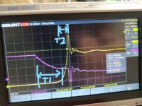
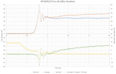
When the lower switch is conducting (current flowing from drain to source) and turns off, the Vds overshoot is 69V with a 40V battery. This is higher and also looks different from Lebowski's 4468 pictures. This is with phase current set at 100A.
I want to double my battery voltage in the future, so want to lower the overshoot.
lower turn off 4p7 15 600ns.JPG

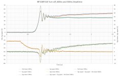
I decreased the deadtime to 500ns, but it looks about the same. Overshoot did go down though to 67V. Is this the right thing to do?
lower turn off 4p7 15 600ns and 500ns.JPG

What parameters should I be looking at? I'd like to understand what the overshoot is coming from. I want to think the main factor is that the current is ramping up through Lp and Q1's diode. But I'm using the same PCB layout and this wouldn't change from using a different mosfet.

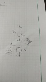
Edit: Read some more stuff, and think this looks like a double pulse test. So the big spike would actually be Q2 turning off as D1 starts to conduct.
drawing small.jpg

Edit2:
I think I need to increase the gate resistors? The reason is that the fall/rise time for this mosfet is faster. Just like how the gate resistors should be bigger for IXTH180, as that mosfet also has faster fall/rise time than IRFP4468.
The higher gate resistance increases time period T2, which is when current is changing from Q2 to Q1's diode+parasitic inductances.
Time period T1 also increases, so I should increase deadtime? Would it be T1+T2, or a bit more or less?
This is with 2x 4.7Ohm turn off resistance on Q2, and overshoot went down to 59.6V :eek:

If I were to keep a 40V battery, would it make sense to use the lower gate resistance to lower switching loss, since the overshoot is under the mosfets 100V rating?

InkedQ1 2x 4p7 ohms turn off resistors resized.jpg

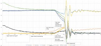
Also, looking at the top mosfet turning off, there's so much going on.. Some pointers here would be much appreciated too. (they don't perfectly line up, off by up to 5ns, as I had to take multiple scope shots and merge them).
Vgs_upper is bouncing up to approximately 3.5V. Is that really bad..?
upper turn off.JPG
 
Lebowski said:
Watch out, the power rating values are only correct for the 100 Ohm example... with 50mA and the voltage you want to drop you can calculate the required rating. 40V and 50mA means you dissipate 2W, the resistor you use should be able to take this . When using 100 Ohm 0.5 W resistors for instance, you need 8 in series for 40V, the 2W dissipation will divide itself equally ove the 8 resistors (so each one will dissipate .25W, well within the 0.5W rating)
Is it 50mA idle or while running?
I'm getting much higher while running.

With a 40V battery, the buck converter was getting a bit hot, 50~60C, without being enclosed in a box. So I replaced my wire short with a 1/2W 100 ohm resistor.

Idle: 5.6V -> 56mA -> 0.31W
However, after running a bit, I noticed the resistor was extremely hot. Measured the resistor while gates are switching, and got
9.8V -> 98mA -> 0.96W

Power to switch the gates:
400nC gate charge * 20kHz * 15V * 6 switches = 0.72W
Battery current:
0.72W / 30V / 80% buck efficiency= 30mA

So my idle (56mA) + gate drive (30mA) through the 100Ohm is already 0.74W. Not sure where the last extra bit is from, maybe the gate driver or microcontroller?

Is my idle current of 56mA too high? Or is that correct, and I just need higher power rated resistors?
The board was a bit difficult to hand solder with the super close components and my thick chisel tip..
 

I can answer some of your questions if you didn't solve the problem yet.
100A is not a few, the measurement and maybe the circuit needs to be optimized. There are serial inductances and radiated coupling from the high current wires and FET pins to the probe. When the current changes there can be several Volts on these inductances (by L*di/dt), and a part of the waveform on the display is that, not the real voltages of the FET.

But first set the dead time so that the turn-off transient is fully finished before the rising of the other FET Vgs starts.
On your first pictures with 4.7ohm it would be 1us or more, on the oscilloscope photo (2x4.7ohm) roughly 2us. Later you can reduce this dead time if there is margin. At higher current and/or higher voltage the turn-off is longer.

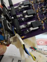
For Vgs and Vds measurements connect the probes directly on the FET pins close to the package, not just somewhere on the GND plane. This excludes the serial inductance from the GND to the FET. The best would be to use differential probes, but normal probes can also be good, but then solder twisted pair wires (10cm or more) on the FET pins with the smallest possible loop at the FET, and connect the probe on the other end of these wires. The small loop minimizes the radiated inductive coupling. If the FETs are fully seated vertically in the board, then the wires can be soldered on the pads on the other side.
The upper FET Vgs and Vds can also be measured the same way, but in every case make sure you connect only one FET at a time to the oscilloscope (Vgs on one channel and Vds on another) and that the controller power supply is isolated from the oscilloscope, and also disconnect everything else from the board (such as a programming cable from a PC), otherwise something will blow up, and don't short the twisted wires accidentally. Then you'll have a clearer picture of the real waveforms.

After that the switching speed, the overshoots/undershoots and the oscillations can be optimized with the gate resistors and RC snubbers on Vgs and Vds.
 
I ended up increasing the gate resistors to 22Ohms and 100Ohms.
Chose 22Ohms to reduce Vds spike to 100V with a 84V battery.
Chose 100Ohms to reduce the Vgs bump I was seeing.
They both seem like way larger values than the other recommended resistors :?

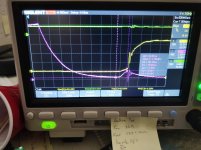
I tried the measuring using the twisted wires, and increased deadtime to 3us.

This is what it looks like:
GATE_LOW low freewheel to high turn-on.jpg
(sticky note's on/off resistor values are swapped)

I'm measuring a 2V bump in the gate voltage. I'm still not sure if this is real or not, or if I can decrease my turn-on gate resistors..
I think I understand that part of that voltage could be due to inductance between my Source measurement point and the actual Mosfet's Source. Since the freewheeling current is decreasing through that inductance, my measurement point would be at a lower voltage, so my measured Vgs might be greater than what the Mosfet sees.
low-side wires.jpg

Edit:
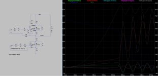
I don't think my measured gate voltage is any good. It didn't make sense to me why my measured Vgs was dropping when Vds was sharply rising.. So tried a simple simulation, and I think the green trace (Vgupper-Vswitch) is what I'm measuring, but the actual gate voltage would be the pink line (Vgupper-Vsupper). They are completely different. I think the Mosfet lead parasitic inductance * dI/dt is what I'm mostly measuring, and this doesn't correspond to the actual Vgs.

ltspice_gate_bounce_sim.JPG
 

Yes, much of the signal is the voltage on the source inductance, and not easy to tell what's the internal Vgs inside the package on the silicon chip. But the current change can be measured independently with a single turn insulated wire loop placed next to the source leg. I used a 10mm diameter circle wire ending also in twisted pair, that picks up 1..3V bumps when the source current changes, and it is comparable with the bumps on the external Vgs. Then it is easier to make a conclusion for the internal Vgs.

The speed of the current change can be slowed down with an external Cgs, that would be C7 in your simulation (and the same on the low side), because it is a negative feedback from the lower end of the source inductance to the gate voltage. Its value is normally smaller than the internal Cgs of the FET. If this cap is added the gate resistors can be reduced, so the current changes are slower, and also the turn-off overshoot voltage is smaller, but the total Vgs transition is faster. But the external Cgs also changes the turn-on waveform, including that it can make the voltage jump on the diode (Vds of the non-switching FET) after the reverse recovery faster and higher, that is not always preferred, so I normally put a small serial resistor with the external Cgs (that's "RC snubber" on Vgs, although it functions as a feedback, not as a snubber). With this feedback a good balance can be found between the switching speed and the overshoot.
 
Back
Top