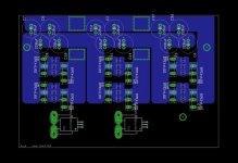
Controller power stage PCB [input wanted]

nieles

10 kW
Joined
Jul 14, 2008
Messages
683
Location
The Netherlands
hi,

i have been designing a Powerstage PCB for my controller build using the controller chip from Lebowski.

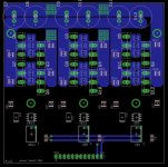
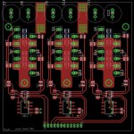
This is what i have so far:
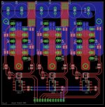
test board fet stage 0.1.6.0 T+B.jpg
test board fet stage 0.1.6.0 B.jpg
test board fet stage 0.1.6.0 T.jpg

and the schematics (its a little messy, i still need to clean it up)
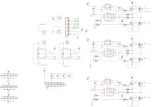
test board fet stage 0.1.6.0 SCH.jpg

as you can see i have been studying this thread 8) : http://endless-sphere.com/forums/viewtopic.php?f=2&t=35071&hilit=water+cooled


few questions:

-What kind of copper pour should i place on the bottomside of the PCB where the fet drivers are located? for optimal noise imunity

-what would be the best way to connect the High power side GND to the GND from the drivers? would it good to use a low value resistor beteen the two grounds?

-i have a dc-dc converter for charging my bootstrap capacitor, are there any drawbacks (other than cost) for using one instead of a diode? in the application notes i have read they only mention the advantages for using one, and not the drawbacks.

Let me know what you guys think!
i am open to suggestions to improve this design
 
It might be better to fit individual gate resistors to each FET, rather than have them share a single resistor. Ideally the gate resistors need to be as close as you can get them to the gate, to minimise the stray inductance between the gate capacitance and the gate resistor. The gate resistor acts to damp the Q of the reactive circuit created by the gate capacitance and the lead/track inductance.

There aren't any drawbacks I've found to using DC-DC converters, they pretty much guarantee that there's always adequate gate drive, no matter what the starting condition. The only downside is the cost.

No reason I can see for not just directly connecting the two ground sides together, either.
 
my $.02,

- I would double the amount of 5181's, use one per FET instead of driving 2 FETs from one 5181.
Two 5181's can share the same DCDC for the high side.
- to minimize the inductance, place the driver <-> FET return wire as close as possible to the signal
wire, so either next to it or opposite on the other copper layer. One of these returns is gnd, so that
one is easy when you do the copper fill. The other return wire is the high side source / low side drain
wire that goes back to the high side driver
- I would put in snubbers :?
 
Jeremy Harris said:
It might be better to fit individual gate resistors to each FET, rather than have them share a single resistor. Ideally the gate resistors need to be as close as you can get them to the gate, to minimise the stray inductance between the gate capacitance and the gate resistor. The gate resistor acts to damp the Q of the reactive circuit created by the gate capacitance and the lead/track inductance.

there is a shared resistor in the positive trace, and a individual resistor in return trace. the idea being help the current sharing beteween the fets by limiting the current through these traces.

i will split up the shared resistor and mount them as close as possible to the fets.

Jeremy Harris said:
There aren't any drawbacks I've found to using DC-DC converters, they pretty much guarantee that there's always adequate gate drive, no matter what the starting condition. The only downside is the cost.

alright good to know! i will keep the dc-dc for now, but also add the necessary traces to use a diode because the controller chip has a function to pulse the lower fets to keep the bootstrap capacitor charged and experiment what i like best.

Jeremy Harris said:
No reason I can see for not just directly connecting the two ground sides together, either.

i was worried i would get extra undershoot at the fet driver if the grounds would be connected together.

should i do anthing special with the 6 input signal pins at the mcu side? to prevent false triggering

Lebowski said:
- I would double the amount of 5181's, use one per FET instead of driving 2 FETs from one 5181.
Two 5181's can share the same DCDC for the high side.

i was thinking of using one "high impedance power buffer" (application note AN-978 p-14) per fet. so in total i would have 4 buffers and 2 ncp5181's per phase.

either this, or using one of these new drivers i found.
irf2186:
http://www.irf.com/product-info/datasheets/data/irs2186pbf.pdf
UCC27211 (this has a bootstrap diode build in, can is still use the DCDC's?)
http://www.ti.com/lit/ds/symlink/ucc27211.pdf

could use only one of these drivers per two fets? or is it more a layout 'thing' to use two drivers?

Lebowski said:
I would put in snubbers
i was hoping i wouldnt need them with this layout, and with some experimenting with different value gate resistors.
but you are right, i should at least add the pads to the pcb so i can add the snubbers if needed!


Thanks for the help guys!! much appreciated

i wont be getting much done on the layout during the week, but i hope i can get a revised layout done in the weekend.

Niels
 
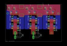
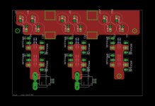
well it took me long enough :p but here is the new layout.
test board fet stage 0.2.2.2 T+B (1).jpg
test board fet stage 0.2.2.2 T (1).jpg
test board fet stage 0.2.2.2 B (1).jpg

the pcb is now 15 by 10 cm

added a lot of copper to the board, but i will also keep the bottom side bare copper so i can build the traces with even more copper.

each fet will get its own driver. the driver will be a power buffer with a p- and n-channel fet. this driver will be situated right in front of the fet, to keep the ringing to a minium.

the power buffers will be driven by a FAN7388 this is a 3 phase fet driver.
 
Back
Top