agree, its not anything of the things i listed. im trying to figure this out.. thinking out loud.
can you remove your clamp circuit (R5, Q5, D6) and just let your driver turn IGBT off at-5V? does this help?
This is a good thing for you to point out.
IN this current build I jumped the clamp Q5 to let the driver hold the igbt off better and It seems worse. So maybe removing the clamp will make it better. I will try this.
R3, R1 are shown as optional. are they populated?
Yes this is needed so the driver can see the voltage and know when to activate the clamp I think
C15 is listed as DNP. did u populate it?
Yes I have a 100nf there
R19, try increase this to 1k ohm. this resistor limits the transient amps that will be pulled out of gate driver IC, this could actually be something related to your problem. you may have to change value of C6 to get same time constant.
OH snap thanks for pointing that out. That's a good one I never thought of...
your turn ON caps C29, C35 this is good. your turn OFF cap, why you have 3x4.7 instead of just two to keep symmetrical? C3 looks like unnecessary extra. don't think this means anything, but it is something that bugged me.
") 7C was worried about a cap on the clamp fet so C3 goes next to the clamp fet
7C was worried about a cap on the clamp fet so C3 goes next to the clamp fet
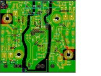
Schottky 5/6 are located in a strange spot. did you really have voltage transients at Vout??
I have 6 schottkies per driver two protecting the signal in 2 protecting the signal out and 2 protecting the signal to the gate of the igbt
R18 seems high, you sure 10k is acceptable?
I will edit this sorry it is a 4.7k I just forgot to edit the sch
this is for leaf inverter, driving IGBT no? this should be turned ON at 15V, not 12V (12 is for mosfets).