simat
10 mW
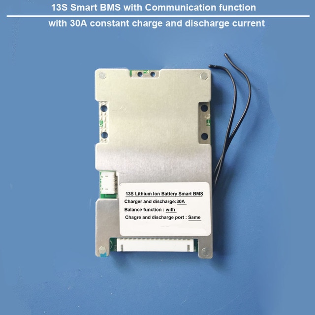
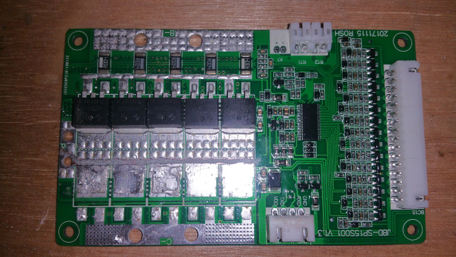
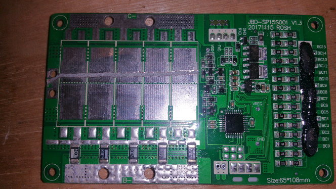
There are a number Chinese Bluetooth PCBs that use the TI BQ76940 BMS controller/controllers connected to an Atmel 8 bit microcontroller looking like this.
One of the main issues with these boards is the layout of the FETs that disconnect the battery from the rest of the world in the case of a fault and the external high current connections.
I have hacked the 30A version of this board to make it a dual port (separate charge and load ports) with ~100A load and ~50A 150V charge ports to connect between a 48V LFP battery with on the charge side 120V solar panels and on the discharge side a 4kW PIP4048 inverter.
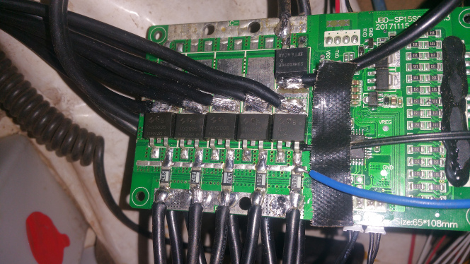
Firstly, I removed the 5 charge FETs
Secondly, I used a Dremel to cut a slot between drains of the charge and discharge FETs to make the BMS dual port. Make sure to cut to the edge of the PCB and check with a multimeter that you have separated the two sets of pads.
Thirdly, I soldered the 5 FETs I removed on the back of the PCB behind the discharge FETs on the front of the PCB. For the discharge FETs
I used 2 Vishay SUM80090E 150V FETs for a maximum charge current of 20A.
To make sure that the current is shared evenly between the FETs and to mininise the interconnection power losses I soldered ~3.5sqmm wires all of equal length from each FET or current sense resistor to 8mm crimp lugs.
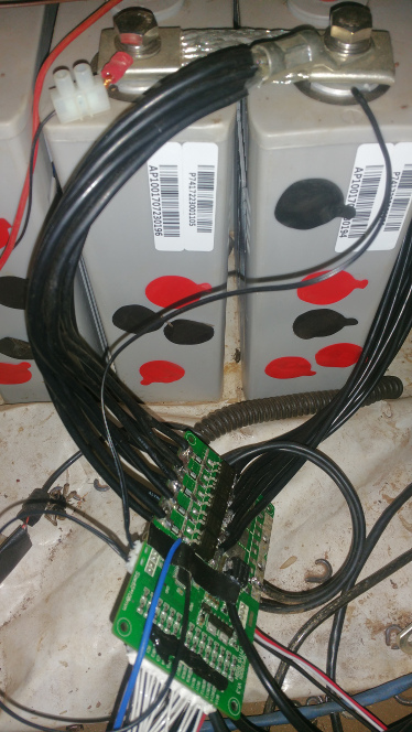
From the voltage drop I measured I calculated the drain source resistance of the original HY3008 FETs to be ~7mOhms, so total resistance of the ten FETs in parallel is 0.7mOhms. This gives a power loss of ~7W with a 100A load.
Simon
One of the main issues with these boards is the layout of the FETs that disconnect the battery from the rest of the world in the case of a fault and the external high current connections.
I have hacked the 30A version of this board to make it a dual port (separate charge and load ports) with ~100A load and ~50A 150V charge ports to connect between a 48V LFP battery with on the charge side 120V solar panels and on the discharge side a 4kW PIP4048 inverter.
Firstly, I removed the 5 charge FETs
Secondly, I used a Dremel to cut a slot between drains of the charge and discharge FETs to make the BMS dual port. Make sure to cut to the edge of the PCB and check with a multimeter that you have separated the two sets of pads.
Thirdly, I soldered the 5 FETs I removed on the back of the PCB behind the discharge FETs on the front of the PCB. For the discharge FETs
I used 2 Vishay SUM80090E 150V FETs for a maximum charge current of 20A.
To make sure that the current is shared evenly between the FETs and to mininise the interconnection power losses I soldered ~3.5sqmm wires all of equal length from each FET or current sense resistor to 8mm crimp lugs.
From the voltage drop I measured I calculated the drain source resistance of the original HY3008 FETs to be ~7mOhms, so total resistance of the ten FETs in parallel is 0.7mOhms. This gives a power loss of ~7W with a 100A load.
Simon
") what do the red and black dots on the side of the cells signify?
what do the red and black dots on the side of the cells signify?