icharger failures, detail how your icharger failed

dnmun said:
if you have a 2596 then install it and see if the power comes back on.
It actually could work if connected in reverse but I have 2 reasons not to do that.
1) I would need to take LM2596 from working step down converter.
2) I am not confident about working with those huge surface mount components.
Would try it only being sure I got the right part.

Meantime, I could use this guy.
file.php
 
Hi Everybody!
First post on ES. I’m also an owner of a damaged Icharger.
In my case it’s a ic1010b+ model and my second unit.
I found this thread while searching for information about it.
And I think it’s a good idea to restart it instead of opening a new one.
This way the information will keep concentrated in the right place.
Well let me describe my crusade.
Yesterday I finished mounting a 4S 5000mAh 40C lipo pack and decided to discharge it @ 7A with an external resistance (extended mode), and charge it to check its capacity. External resistor adjusted according to the formulae in the manual, everything correctly connected and I pressed the Start button. The display showed the current increasing up to 7A and decreasing to 1,6A, when I stopped the process. After a double check I tried again.
Suddenly the magic white smoke smelling burned epoxy and semiconductor came form the fan. I switched off my power supply immediately but the damage was already done.
I adjusted the current limit of CC-CV power supply to 300mA (enough to power the unit) and connected it for safe test. The current limit led bright up showing a short circuit.
Send it to Junsi for repairing or not? Well I decided to open and inspect the circuit.
Transistor Q29 (SS8050) toasted and U3 (mosfet IRF3205) short circuit. I opened my also damaged old ic1010b and removed the components above to fix the newer unit. Damaged components replaced, I decide to repeat the safe test. It starts OK!
I connected a small 2s 300mah pack to its output and balance port. Adjusted 100mA charging rate and pressed start button. Message “Please wait” as always, the current slowly increase on display of power supply monitor, but followed by an error message – Connection Breakdown – and the process stopped. Too early to commemorate!
Time to a second inspection but now I carefully checked all the semiconductor components. First, all the mosfets were removed from the board and checked one by one. All of them are apparently ok but they seem to present Overheat Stress.
After that, it was time to check all the small sot23 transistors. The suspicious ones wereremoved from board for functional test. Q32 and Q43 (mosfet 2N7002) were damaged and were replaced by good ones from old ic1010b unit.
Now here I am kindly asking for help from the more experienced people here before moving to my next step: solder the power mosfets back to the pcb and repeat the safe test or replace the already used power mosfets by new ones??
I used my multimeter on OHM function to switch the power mosfets irf3205 ON and OFF through the gate pin but each one presented different resistance value between source and drain pins, varying from 28 to 40 ohm. Exception to power mosfet U7 (IRF1404) with 4.5 ohm.
Maybe are they stressed by overheat?
Here is the picture of the smd component from my “somewhat” disassembled PCB.
Despite my language limitation, I hope my information was clear enough to enlighten the failure.
Any questions or comments are welcome I will really appreciate any help.
 
'connection break' can happen when the output voltage exceeds a fixed level i think. that has happened to me on the imaX B6.

otherwise it could be the mosfet on the output burned open circuit but it sounds like you were able to discharge for a brief time.

can you show the other side where the transistors are located and indicate which ones you replaced?

there is not need to scrap another one for parts since these mosfets are common and many of us have them laying around if you just ask for them.
 
Thanks Dennis.
In fact I didn't remember the correct error message and unfortunately I can't repeat the test because the power components were already removed.
Yes, I could run all the menu and at least perform a discharge cycle but the inicial ramp up of discharge current was weirdly slow, not as used to be.
Besides that, I tried to check the internal resistance of my small lipo battery pack but the display showed "zero" miliohm for all the 3 cells.
It means that the circuit was not capable to drain any current to measure the voltage drop and calculate the internal resistance.

Regarding the damaged componentes, here is a more detailed list:

- U3: N-channel Power Mosfet IRF3205 (it is pair with U1, another IRF3205);
- Q29: NPN transistor SS8050, marked on the body Y1 (it is pair with PNP transistor Y2 SS8550 Q36 to form the driver circuit for U3, I supose);
- Q43: N-channel fast switching mosfet 2N7002 (commonly used as a gate driver for power mosfets, according to datasheet)
- Q32: same 2N7002, but I'm not sure it was damaged by the malfunction or by my soldering iron;

Note:Those are the damaged componentes identified till the present moment. I attached below a more detailed picture with location of damaged components highlighted in red square.
Luckly there's no sign of open cooper traces on pcb. The cooper traces are thick due to high currents present in the circuit.

Well, I can identify the circuit blocks of the charger but I don't understand the specific function of each one.
I see U7 (IRF1404) as a voltage step up circuit, The pair U1/U3 (IRF3205) as a voltage regulator (?), the pair U2/U4 (IRF3205) as a current regulator ( :?: ). Please corrrect me if I'm mistaken.
I know it's more complex than this because this charger has regenerative function and can discharge a battery pack connected to the output awhile charges a car battery connected to the input, in example.

I've commented in my last message that the multimeter test to check power mosfets U1 to U6 (IRF3205) showed very different results for measured Source-Drain resistance during ON state, varying from 36 to almost 90 ohm (not miliohm). I understand that the voltage present on the multimeter is not enough to switch a mosfet ON completely, that could be the reason for such a high S-D resistance, wright? But why so different readings?
I'm thinking seriously about replacing all IRF3205 (U1 to U6) by new ones.
Pictures of both sides.
 

Attachments

  • IC1010B+ Charger - Shorted Components.jpg
    IC1010B+ Charger - Shorted Components.jpg
    227.2 KB · Views: 4,270
i doubt if you can measure S-D resistance that way and it is not important to know either. i always recommend just verifying that the body diode is intact and the forward bias of the body diode is similar in all the mosfets with the same part number.

but where is the fuse? did you test it for continuity before you removed it?the shunt wire R5 is the thing i usually expect to be burned open when people discharge their pack through the icharger. it just gets too hot and melts but yours looks intact.

the boost converter uses that inductor to push current up to a higher voltage so that the higher voltage can be applied to the terminals of the pack. the two adjacent 3205 are the switching mosfets that allow the current to come in from the power supply and then turn off as the flyback pushes the current out of the inductor to the output.

all of those small TO223 parts are the gate driver circuit and the big 48 pin IC controls how much they have to work to keep kicking juice through the inductor.

U8 is the voltage regulator i think for the 5V supply to the big IC and if it failed then nothing would be illuminated or work so it is ok.

i doubt if you have any burned traces either since i see none and that is not a likely failure imo.

hard for me to see on mine right now but i will look more during the day when i have more light and i can see better.

to test your nchannel mosfets just use the diode tester. put the red probe on the drain and the black probe on the source and it should be open circuit. reverse them and put the red on the source leg and the black on the drain and you will see the body diode forward bias. all of the 3205s should be identical in forward bias.

check resistance between gate and drain or source to verify the gate has not punched through but i doubt it will be damaged if the body diode is intact.

and you can use the diode tester to push current onto the gate, red don gate, black on source, then quickly switch the red probe to the drain and you should see the resistance of the channel increase as the gate voltage bleeds off.

i have two here i tried to repair for greg but ruined them because my hands shake so much now but i should be able to test different circuit parts on it to verify for you if you need second source.
 
Hi Dennis. Now I coming back here earlier (free time in my job). Time zone never helps us.

dnmun said:
i doubt if you can measure S-D resistance that way and it is not important to know either. i always recommend just verifying that the body diode is intact and the forward bias of the body diode is similar in all the mosfets with the same part number.
You're wright. I could get 8 good mosfets IRF3205 from both chargers and the forward bias is ok on all of them. Thanks for the info.
but where is the fuse? did you test it for continuity before you removed it?the shunt wire R5 is the thing i usually expect to be burned open when people discharge their pack through the icharger. it just gets too hot and melts but yours looks intact.
The fuse is Ok. I removed it to have better access to the transistors located behind it. It's better to remove than moving up and down and finish broking one of its terminals.
the boost converter uses that inductor to push current up to a higher voltage so that the higher voltage can be applied to the terminals of the pack. the two adjacent 3205 are the switching mosfets that allow the current to come in from the power supply and then turn off as the flyback pushes the current out of the inductor to the output.
So it is a powerful DC-DC voltage step up circuit. And there's the third pair U2/U4, but they were not damaged. Mosfet U2 was damaged on my old ic1010b while discharging a 6S lipo pack, what means that this pair is probably used for the discharge cycle. Things start to make sense...
all of those small TO223 parts are the gate driver circuit and the big 48 pin IC controls how much they have to work to keep kicking juice through the inductor.

U8 is the voltage regulator i think for the 5V supply to the big IC and if it failed then nothing would be illuminated or work so it is ok.
The shorted mosfet U3 probably caused overheat of Q29 frying it and also damaged mosfet Q43 in cascade. I will check code of IC U8 to know its function.
i doubt if you have any burned traces either since i see none and that is not a likely failure imo.
The dark green color of pcb didn't permit me to see if the pcb is even multilayer, what I suppose not to be the case.

hard for me to see on mine right now but i will look more during the day when i have more light and i can see better
My glasses and the artificial light are not helping me either :lol:

to test your nchannel mosfets just use the diode tester. put the red probe on the drain and the black probe on the source and it should be open circuit. reverse them and put the red on the source leg and the black on the drain and you will see the body diode forward bias. all of the 3205s should be identical in forward bias.
check resistance between gate and drain or source to verify the gate has not punched through but i doubt it will be damaged if the body diode is intact.

and you can use the diode tester to push current onto the gate, red don gate, black on source, then quickly switch the red probe to the drain and you should see the resistance of the channel increase as the gate voltage bleeds off.
Exactly what I did to test my fets. Lesson learned from the time I used to repair switched power supplies.
i have two here i tried to repair for greg but ruined them because my hands shake so much now but i should be able to test different circuit parts on it to verify for you if you need second source.
Thanks for your support Dennis. I will finish testing the transistor and diodes from the gate driver circuits and once I'm confident everything is ok, I will resolder the used but selected power mosfets for a second run on my power supply with current limitation. Let's see what happen. Wish me luck. :)
 
Well, I have good and bad news.
Yesterday I finished the verification of all transistors and fets used in the driver circuits.
I resoldered my good power mosfets 3205 and verified if the solder didn't cause any bridge on their terminals.
Everything ok, I ajusted my power supply to 12V with current limitation of 400mA and connected the charger.
I connected my small 3S lipo pack and its balance port to the charger.
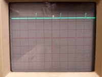
This time I started the tests by performing a charging cycle with current adjusted to 100mA.
IT WORKS !!! :D :D :D
I started the internal resistance test. Perfect! It displayed the resistance of all 3 cells in the lipo pack.
But here finishes the good news.

I decided to perform a discharge cycle with current adjusted to 100mA.
When I pressed the Start button the charger started the same weird very slow ramp up current which increased till 100mA and falled down to 40mA.
Suddenly the smell of burned component came from the charger again! :x :(

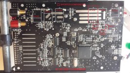
I disassembled the charger and a fast initial analysis showed that the same components were shorted.

But this time a smd resistor toasted and the printed value on its body became unreadable.
It is located between the pins of Q40 and Q43, the unique resistor diagonally soldered above the printed mark R104 on pcb.
I could measure 53 ohm but the value could have changed after the overheating...
My prevous picture doesn't have enough resolution to show its value.
Does anybody have an open IC1010B+ to tell me the printed value on the body of this resistor?
P.S.: the picture is attached below.
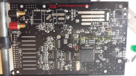
I decided to follow the traces from both gate pins of fets Q43 / Q32 and discovered that both are directly connected to the output pins of IC U13 without any means of overcurrent protection like resistors or diodes. That's bad!


IC U13 (which seems to be a microcontroller) had its printed code erased. :evil:
It probaly controls the discharge process of ic1010b+.
Connected to IC U13, there's the transistor Q49 (a smd shunt regulator LM431) also shorted between pins 1 and 3. (probably damaged during the first failure and not replaced on the subsequent repairs...). What is the function of 431? Voltage regulator? Comparator? Voltage reference?
I suppose it is a voltage regulator dedicated to feed the microcontroller U13 but difficult to guess its real function. Please correct me if I'm wrong.

When the fets became shorted, the overcurrent probably shorted shunt regulator Q49 (431).
My fear is that the output pins of IC U13 were also damaged by the overcurrent and any trying to repair this charger will be a waist of time.
But I'll give my ic1010b+ another chance.

The initial shop list for damaged components:
- U3 power mosfet 3205
- Q29 smd npn transistor 8050
- Q43 and Q32 smd n-channel mosfets 2N7002
- smd resistor with unknown value (?)
-Q49 smd shunt regulator 431

This list is result of a fast inspection and more damaged components can show up.

Now I have to buy replacement parts because I don't intend to continue scraping my old ic1010b charger.
New parts will be here probably at the middle of next week.
I have attached a picture below to show the "new" damaged components highlighted in red, besides the ones showed in the previous picture.
The paths from IC U13 to Q32/Q43 highlighted in yellow. And the fried smd resistor in green.
More to come.
 

Attachments

  • new damaged components.jpg
    new damaged components.jpg
    211.5 KB · Views: 4,263
431 family is called a voltage reference and the cathode is held to a specific voltage which if i recall correctly is 2.495V? and the R129 is labeled 240 or 24 ohms.

R104 and R109 are labeled 473 or 47kR.

the ping v1 signalab BMS uses the 431 for the voltage reference. so i have those too. it may be TO23 and not the 223 part though.

why do you think the transistors have failed?

U13 is the display driver.
 
Hi dnmun! I'm back with more info.
Replacement components will be here probably begining of next week. I've ordered extra components to repair my old 1c1010b, and ic208b+ from a friend.
dnmun said:
431 family is called a voltage reference and the cathode is held to a specific voltage which if i recall correctly is 2.495V? and the R129 is labeled 240 or 24 ohms.
Thanks for the valuable info dnmun! The toasted resistor doesn't have any identification on my pcb. It's simply soldered between Q40/Q43, maybe as a fuse in case of short circuit. I suppose this will be the most difficult component to get because they don't use to sell resistors in small quantity. I'll look for it in old pcb's at my job. Even two 47R resistors in parallel can solve my problem.

TL431 smd is sot23 case . As I commented before, it was damaged in the first original failure and I didn't realize it. this component is damaged on both ic1010b+ and ic1010b. It seems that it normally fails in case of a short circuit in the power stage, during a discharge cycle. I've already ordered some units for replacement.

the ping v1 signalab BMS uses the 431 for the voltage reference. so i have those too. it may be TO23 and not the 223 part though.
why do you think the transistors have failed?
The first failure I really don't know what caused it, but the subsequent failures during the discharge test are related to the not replaced 431.
U13 is the display driver.
I agree with you but two pins from U13 are directly connected to the gate of Q32 and Q43 (fets 2N7002) what makes me think that U13 controls the discharge cycle through those gate driver fets.
 
i was wondering how you tested the transistors in order to know they had failed.

did you measure the 24R surface mount with your DVM directly? it may have only overheated and is still intact. i can compare the measured value to the one i have here if you need a reference.

yes, you are correct, SOT23, not TO23 duh.
 
dnmun said:
i was wondering how you tested the transistors in order to know they had failed.
For NPN and PNP transistors, I adjust my multimeter to diode test and measure the forward and reverse bias on the three terminals of transistor. If one of them is suspicious or difficult to measure due to other components interfering with the readings, I remove and test it out of pcb. Regardinghe n-channel fets from driver circuit, I check forward bias diode and, in case of doubt , I remove from pcb and test them as commented some posts before.

did you measure the 24R surface mount with your DVM directly? it may have only overheated and is still intact. i can compare the measured value to the one i have here if you need a reference.
Yes, I measured it directly on pcb and the value was 53 ohm. But I must inform you that it really "fried". The printed value on its body is totally blurred. I checked the pictures taken before it fries. The resolution was not good but it seems that the first digit is "2" and the rest is unreadable. My old IC1010B has a 24R resistor well identified on pcb, but the engineer from Junsi apparently forgot to reserve a place in the IC1010B+ pcb layout to solder the 24R on and soldered it over the pins of Q40 (nfet 2n7002) and Q43(npn transistor 8050) . Please check the last pictures and you'll know what I mean.

Now I'm waiting for replacement parts.
 
The replacement componentes arrived last Friday.
Meanwhile I could open the IC208B from a friend of mine.
The unity is working ok but the display shows random characters on the upper line of 2x16 lcd display. I'll try repair it later.
I opened 208B to check the output signals of pins 30, 31 and 32 from microcontroller U13 which send the pulses to control power circuit of mosfets U1 and U3 (IRF3205).
Those three pins are connected to pull-up 20K ohms resistors to assure 5 Volts for high level phase.
Pins 30 and 31 of U13 are connected to gate pin of fets Q32 and Q40 (2N7002).
I put the 208B to charge a 3S lipo pack @ 100mA and connected my oscilloscope to the pins 30 and 31.
The oscilloscope is adjusted to 2V/division.
They are PWM complementary signals to control the output voltage from charger to the lipo pack through power mosfets U1 and U3 (IRF3205).
Here are pictures from oscilloscope's screen.
 

Attachments

  • charging signal of pin 30-U13 IC208B charger.jpg
    charging signal of pin 30-U13 IC208B charger.jpg
    56.4 KB · Views: 4,176
  • charging signal of pin 31-U13 IC208B charger.jpg
    charging signal of pin 31-U13 IC208B charger.jpg
    48.3 KB · Views: 4,176
Continuing...
I repaired the IC1010B+ again by replacing fet Q40 (2N7002), and soldering the 24R smd resistor borrowed from old IC1010B board.
The other componentes were ok.
I connected the 101B+ to the power supply and it was working ok.
I wouldn't repeat another discharging test for sure. :roll:
I adjusted a charging cycle @ 100mA and connected the 3s lipo and balance port.
While pressing the start button I put my finger over the driver circuit of power mosfets U1 and U3.
I noticed that Q40 (2N7002) and 24R resistor warmed a lot but stayed cool after some seconds when the charging started itself.
My conclusion is that the charger performs a fast discharging at the begining of the process to analyze the battery's health.
Luckly nothing was damaged and the charging worked ok.

during the charging I connected the oscilloscope to pins 30 &31 of U13 to compare the signals of IC208B.
And here comes the results: pin 31 from CI U13 of my 1010B+ is damaged.
Let's compare the signals:
 

Attachments

  • charging signal of pin 31-U13 IC208B charger.jpg
    charging signal of pin 31-U13 IC208B charger.jpg
    48.3 KB · Views: 4,176
  • charging signal of faulty pin 31-U13 IC1010Bplus charger.jpg
    charging signal of faulty pin 31-U13 IC1010Bplus charger.jpg
    51.3 KB · Views: 4,176
My conclusion is that the first original failure caused by the discharging process (with external resistor) shorted fet U3 (IRF3205), Q43(8050) and Q40(2N7002).
The overcurrent caused by the shorted Q40 damaged pin 31 of microcontroller U13.
Observing the last pictures, the signal of pin 31 from IC1010B+ is not pulsing to low level as IC208B, what confirms that the internal circuit of pin 31 is damaged.
And, even with a faulty signal from pin 31, the ic1010b+ surprisingly works!
Logic & Driver circuits from IC1010B+ and IC208B are identical.
After opening 208B I could realize that the printed code on U13 body was not totally erased.
Typing the code on internet browser I made my best discovery.

Microcontroller U13 is an ATMEL ATTINY461-20MU-32M1-A (datasheet)

It's a in-circuit-programmable Low Power 20MHz 8-bit AVR Microcontroller from Atmel, packaged in a tiny 5x5x1mm 32 pin case.
This microcontroller has a central soldering pad located under its body, probably to improve heatsink performance.

The bad news are that it demands specialized tools to remove it and it's not locally available to me .
I'll take a look at Ebay or Aliexpress.

Picture taken from IC208B.
 
I have an icharger 1010b+ that has been working well for about 3-4 years. When I plugged it in to charge a 6S 30Ah battery at 7.5 amps, after about 10 seconds it gave the error "internal temp too high" and within about 1 second the screen went blank. It wouldn't turn back on, it clearly wasn't overheated. I tried different power supplies, and it just would not turn on, the screen would remain blank.

I was just about to buy a new charger when I tried one last desperate attempt to save it. I plugged it into the USB port on my laptop, downloaded the firmware updater and ran it, and after about five minutes, the screen came back on and it works again!

I don't know what happened to it so that it wouldn't turn on, but updating the firmware seemed to fix it. To be honest, I think I did have the latest firmware, so I didn't update the firmware, I just reinstalled it.

Good luck to others with ichargers!
 
My icharger 3010b failed in a way I have not seen here before. I connected it to charge a 10S lipo pack as I always do, and it would not do a balence charge because it is reading a false low voltage on cells 7 to 10 ( about 2.7 volts if I remember correctly ) . I checked the cells with a volt meter, and they are not not out of range, all cells are about the same. For some reason it just started sensing a low voltage on the last 4 cells. I opened the charger up, and there are no visable fried parts, no smell, nothing unusual. I re-flashed the firmware hoping that the charger memory became currupt , but that didn't help. The voltage calibration feature is not able to correct the huge error either. Looking at the readings in monitor mode seems to show more than normal 'noise' on the readings on the low readings as well.
The overall pack voltage does display and work correctly, I can bulk charge fine with the charger. I just can't balence charge.
Does anyone know if the 3010b uses more than one ADC on the cpu, and maybe the second one is defective ? I ordered some spare analog multiplexors, if I can confirm if one of them went bad.
I wish I had a circuit diagram !
Thanks for any help or hints.
 
Dr.Feelgood said:
I have an icharger 1010b+ that has been working well for about 3-4 years. When I plugged it in to charge a 6S 30Ah battery at 7.5 amps, after about 10 seconds it gave the error "internal temp too high" and within about 1 second the screen went blank. It wouldn't turn back on, it clearly wasn't overheated. I tried different power supplies, and it just would not turn on, the screen would remain blank.

I was just about to buy a new charger when I tried one last desperate attempt to save it. I plugged it into the USB port on my laptop, downloaded the firmware updater and ran it, and after about five minutes, the screen came back on and it works again!

I don't know what happened to it so that it wouldn't turn on, but updating the firmware seemed to fix it. To be honest, I think I did have the latest firmware, so I didn't update the firmware, I just reinstalled it.

Good luck to others with ichargers!

I had the same experience with my 108b. Was working fine until one day only displayed hash marks. Updated software over USB and came back to live. This seems suspicious to me what with dr Feelgoods experience with his 1010b- i.e. Possible built-in obsolescence?? Please chime in.
 
An update on my 3010B which was showing incorrect low volts on cells 7 to 10. ( 2.6 volts instead of 4.2 , well out of CALIBRATION range )

I bought another one, which worked for 6 mo. , and now this new 3010B is doing the same thing, after 6 mo. !!
I can't balance charge, since it thinks the cells are way out of whack, which they are not.
I thought I would have time to debug/trace signals with the new charger, but I didn't get to it, so now I have two defective chargers.
I did some circuit tracing with a scope, and it looks like one of the quad opamps powersupply zener shorted out. The second opamp has a similar looking Zener, which I think is 22 volts, but when I replaced the shorted zener ( with a 22 volt one ) , the readings for cells are all over , mostly too high , some hitting 5 volts reading. Odd thing is the values of the first 6 cells are also messed up with the second zener replaced.
Diode 15 is the one I replaced.

Does anyone know what the correct zeners values should be ?
The design of this charger looks rather convoluted making it hard to know whats going on, circuit wise.
Perhaps someone here who can get to the circuit can offer some help. Gone are the days of openly available circiuts so you can fix things ... oh well.
 
dudewheresmycar said:
An update on my 3010B which was showing incorrect low volts on cells 7 to 10. ( 2.6 volts instead of 4.2 , well out of CALIBRATION range )

I bought another one, which worked for 6 mo. , and now this new 3010B is doing the same thing, after 6 mo. !!
I can't balance charge, since it thinks the cells are way out of whack, which they are not.
I thought I would have time to debug/trace signals with the new charger, but I didn't get to it, so now I have two defective chargers.
I did some circuit tracing with a scope, and it looks like one of the quad opamps powersupply zener shorted out. The second opamp has a similar looking Zener, which I think is 22 volts, but when I replaced the shorted zener ( with a 22 volt one ) , the readings for cells are all over , mostly too high , some hitting 5 volts reading. Odd thing is the values of the first 6 cells are also messed up with the second zener replaced.
Diode 15 is the one I replaced.

Does anyone know what the correct zeners values should be ?
The design of this charger looks rather convoluted making it hard to know whats going on, circuit wise.
Perhaps someone here who can get to the circuit can offer some help. Gone are the days of openly available circiuts so you can fix things ... oh well.
Is there any chance that the balance wires on your battery are shorting and that is causing the repeatable issues you are seeing in Your 1010? The Jst-xh wires connectors used are so tiny it’s conceivable that the wire from say cell 4 is sparking or shorting to cell 3’s connector. The charger would certainly be confused by what voltage it saw, but could it hurt the charger?
 
I don't think it's caused by shorted wires. I believe it's because a 10 cell charger has some design requirements to handle the high voltage. The zeners look like they are used to drop the voltage to the Vcc of the opamps. I only use the charger for my 10 cell bike battery. I think it is a weak design, frankly. The design looks wacky, there is a 8 to 1 analog mux, a dual 4 to 1 mux, and two quad opamps. Some tricks are being used to get 10 channels of reading, there are some transistors scattered around to steer some signals as well. Maybe they are trying to save $1 on parts costs, I don't know.
I think it's funny they grind off the ID of the CPU and one other chip.
All I know is D15 , a zener, is shorted causing one of the opamps to have Vcc near ground. Maybe that opamp fried as well. The opamps are usually used to read the voltage difference between cells.
Maybe there is a repair person in the EU that can fix both of the for me ? I'm not shipping them to the states.
I'm holding $400 of defective charger, and a $0.20 part may be the fix .

So , if anyone knows what the spec. for Diode 15 is, It would help.
 
dudewheresmycar said:
I don't think it's caused by shorted wires. I believe it's because a 10 cell charger has some design requirements to handle the high voltage. The zeners look like they are used to drop the voltage to the Vcc of the opamps. I only use the charger for my 10 cell bike battery. I think it is a weak design, frankly. The design looks wacky, there is a 8 to 1 analog mux, a dual 4 to 1 mux, and two quad opamps. Some tricks are being used to get 10 channels of reading, there are some transistors scattered around to steer some signals as well. Maybe they are trying to save $1 on parts costs, I don't know.
I think it's funny they grind off the ID of the CPU and one other chip.
All I know is D15 , a zener, is shorted causing one of the opamps to have Vcc near ground. Maybe that opamp fried as well. The opamps are usually used to read the voltage difference between cells.
Maybe there is a repair person in the EU that can fix both of the for me ? I'm not shipping them to the states.
I'm holding $400 of defective charger, and a $0.20 part may be the fix .

So , if anyone knows what the spec. for Diode 15 is, It would help.

Well that sucks. I wish I had the answer for diode 15 for you.
10 cell chargers are not very common either so the 1010 was an easy pick for me for its relatively lower price for a 10cell charger and now I have to look forward to the likelihood that the charger will fail!
 
Just an update, I replaced the d15 zener that powers the lower opamp with a 43 volt zener. Now the opamp has power . This corrected the voltage readings on cells 7 to 9, but cell 10 is still reading high. So now it's a 9 cell balance charger ;). I fear that the opamp does not get used to read cell 10, and maybe that cell is read by a seperate ADC of the CPU. Sure wish I has a circuit for this POS charger. So hard to trace signals ! Not an elegant design, I can say that for sure. *sigh*
 
My 1010+ is dead. Overvolt in input plug. (43v)
Any suggestion about resurrecting it?
Caps are not enlarged and I think the problem can be some MOSFET.
Someone knows if Junsi can save me?
My charger is 6/7 years old. Always perfect but first "S" has ever wrong IR measure. 50ohm in eccess.
 
Found this thread via Google, registered to share my findings as well!

I have a 208B that had been a workhorse, never an issue. Actually I've been using it with a homebrew reverse E-bike generator, a 24v brushless motor fed to a home-made Schottky bridge rectifier, a big cap bank, then the iCharger 208B feeding a 6S LiPo pack. Makes for an excellent exercise rig. I try to go for 4Ah per day and discharge the battery into my OmniCharge, in turn to charge anything else (laptop, phone, etc).

Unfortunately, I blew it out by connecting it to an unregulated DC motor on a hand-crank, and at open circuit, it exceeded the 32V input voltage limit and blew out that DC-DC controller IC on the input with its ground-off markings.

With my own research, I found that I could connect to the little 4.3v/470uF capacitor under the LCD and feed it 5 volts (I tried 3.3v at first, not knowing what its internal logic level was, but found it didn't light the display), and it powers up fine - just like the previous post and a few others. I tried replacing it with an LM2596 and applying low voltage to the input (5.3v) which should power it up but not blow anything out if it's a dead short... nope, no current draw, no lights, no voltage at that capacitor. Doesn't seem to have done the trick.

I'm curious about replacing that input logic supply with a 12v/5v dual voltage converter... maybe that could be the solution? I guess I'll have to poke around to find where the 12v gets applied, but a capacitor somewhere will probably hold the answer.

TL;DR: Nope, not an LM2596.

Update: OK, I tried applying both +5v and +12v aside from the bulk supply voltage and the battery. Still no output (connection break error when trying to start; no current drawn from bulk supply). Used a USB boost DC-DC converter module to provide the 5v/12v from a USB supply, and a bench power supply set to 12v for the bulk power. Applied the 12v to C51 (small green capacitor near the input, 25v rated), and applied 5v to C10 (under the display). No love :(
 
OK, I got that iCharger 208B working again. I had bought an iCharger 3010B that I screwed-up with a brief reverse polarity (ugh...), now it doesn't start charges anymore - it just crashes and reboots when it does "battery check / please wait".

So I stole the 3010B's 5-pin regulator IC and slapped it in the 208B ;)

Success! Fully and completely back to life, everything works exactly as it should. Now this iCharger 208B has lived 3 lives!

So, that IC is all that's the fault with an over-voltage blowout (as long as it was minor over-voltage). I went on Mouser and picked out a couple sample TO-263-5 chips that have different pinouts from the LM25*6 series. Figured I'd group them in with an order where I'm also buying an OLED character replacement screen for the iCharger, since I damaged my original screen trying to remove it - and OLED on an iCharger is going to look sexy as heck.

update: don't buy that oled display. it doesn't work with the iCharger. ask me how I know. -_- It's designed to emulate the same Hitachi controller every character LCD is based on, but it has flaws that break compatibility in weird ways. I got a white-on-black LCD instead, still looks pretty cool but it's slightly fatter (0.5-1mm) than the original so it was a hell of a squeeze. Well, at least it works and it looks nice doing it.

update: aaaand none of the ICs I picked worked in the 3010b either. So it's still an open question what that IC is. Don't understand why they ground off the markings on it. Maybe it's not a single-chip converter after all, since there's lots of additional circuitry there. I guess the next step would be to try shotgunning various chips in TO-263-5 packages that might make sense. Might be a totally bespoke circuit that enables it to create multiple DC outputs (5v, 12v) from a variable input.
 
Back
Top