Snubber Design for Controller Choice of Capacitor and Power

glenn0010

100 W
Joined
Jul 1, 2015
Messages
117
Location
Mgarr, Malta
Hi All I am desgigning my own 3 phase motor controller. I want to implement a snubber circuit to Protect the FETs. I will use and RC snubber circuit since it is simple and effective, even though it has quite low efficiency (approx 40%-60%).

I have found this application note which is great and guides you through the process of designing the snubber effectively. I have understood all the process however I still have some unanswered questions.

https://assets.nexperia.com/documents/application-note/AN11160.pdf

1 - Do the snubber capacitors (i.e. C add for testing and the final Cs) need to be LOW ESR etc since they are more expensive. I think so as the ringing frequencies can be in the MHz ranges so an electrolytic will be too 'slow' to react.

2 - How do you calculate the power rating that the resistor is required to be since it dissipates heat in it?

3 - In page 8 the application note states the following :
"As seen in Figure 6, the snubber has almost eliminated the ringing in the VDS waveform.
This technique could also be applied to the MOSFET in the Q2 position."


I am assuming that from that statement I need a subber across both the high side and low side FETs at the same time. If this is correct, can I assume the snubber values are the same as those calculated for the high side FETs since the positioning on the PCB of the FETs maybe different hence leading to a different Llk (stray inductance). However I think this would have minimal affect.

Thanks for your help !
 
Hello.

1) I would not bother with low ESR capacitors because an RC snubber is already adding resistance in series with the capacitor. Going with low ESR capacitors would mean you need to add higher resistance in series to compensate. Unless you calculate that the capacitor ESR gets significantly high (really shifts the total series resistance), regular capacitors should be fine. I haven't checked, but I would think that the capacitance values for this kind of snubber would be low enough that you could be using ceramic capacitors.

2) To calculate the power rating, what I've done before is simulate the circuit over one full period of the switching cycle. I exported a table of the voltage/current across the resistor, and then put it in excel so that I could calculate the instantaneous powers and then average all that to get the power dissipation. You could also just estimate it and select a resistor that's probably bigger than you would need.

3) I don't think it means that you could use the exact same values, but you would probably do fine with those.
 
1) You're right about the size of the ca0s. In the example give and others I've looked up the sizes are small so it is not a problem.

2) So after determining the parasitic cpaacitance and inductance, I can stimulate the circuit with those values and determine the power rating required.

3) So as expected, I need a snubber for the high side and a snubner for the low sode correct?


Thanks so much for your help!
 
glenn0010 said:
So as expected, I need a snubber for the high side and a snubner for the low sode correct?

I think you would do well with snubbers between the bridge outputs and ground, this seems to be the most common arrangement. I can't find much information about snubbers across each switch in a bridge. Take a look at the recommended snubbers for this MOSFET block by TI: http://www.ti.com/product/CSD88599Q5DC/datasheet/layout

It also depends on the power level of your controller and the physical layout. Do you have any more details about the application of your controller, or your design targets? What kind of power supply are you using? You might want to watch out for inductive spikes on your main power input as well.
 
Addy said:
glenn0010 said:
So as expected, I need a snubber for the high side and a snubner for the low sode correct?

I think you would do well with snubbers between the bridge outputs and ground, this seems to be the most common arrangement. I can't find much information about snubbers across each switch in a bridge. Take a look at the recommended snubbers for this MOSFET block by TI: http://www.ti.com/product/CSD88599Q5DC/datasheet/layout

It also depends on the power level of your controller and the physical layout. Do you have any more details about the application of your controller, or your design targets? What kind of power supply are you using? You might want to watch out for inductive spikes on your main power input as well.

Hi thanks for the reference, I have read the datasheet you link and found the snubbers you are talking about. Now I am bit confused as to where to apply them, across high side fet only, low side fet or across both ?
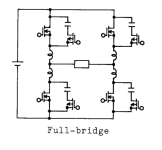
I am thinking it should be applied across both since I do not want to experience ringing and voltage spikes across either of the Fets. For context, I will be switch the high side FET using PWM across it while the low side FET will be kept constantly on (of course not of the same phase).

View attachment 1

Capture1.PNG

While reading a paper I stumbled across this, which shows a switched snubber circuit across both the high and low side FETs however no description about it was given. Granted it was a switching snubber however I think the concept is the same. I am leaning towards doing a snubber across both FETs just to be sure, (couldn't hurt right?). I think this is a good option since you have stay inductance and capacitance for each FET as shown in the diagram

As regards to the power etc. 48V Battery, 1kW Motor around 20A current limit. I have already made a project about this however it was very expensive since I used 6 isolated DC/DC converters to drive the FETs. I m doing this current project for my thesis and I am focusing on optimizing the hardware design and looking in details at the waveforms. The link to my thread can be found here:

https://endless-sphere.com/forums/viewtopic.php?f=2&t=88113&start=25
 
Back
Top