
It looks really good!thorlancaster328 said:The current sensors I use in my design (MLX91220 - https://www.mouser.com/pdfDocs/MLX91220-Datasheet-Melexis.pdf) can detect a short circuit in 2 microseconds, which will result in the FET turning of in under 3 microseconds with hardware fault detection (no ISR).
You are using an out of date browser. It may not display this or other websites correctly.
You should upgrade or use an alternative browser.
You should upgrade or use an alternative browser.
10kW BLDC motor controller up to 90V and 200A with sensorless FOC - build thread
- Thread starter peters
- Start date
mxlemming
100 kW
- Joined
- Jul 17, 2020
- Messages
- 1,122
I take it back, your desat probably will work just great then.
How about VESC 75 and VESC 100? No drv on them... Can't find any protection in the schematic. I'm getting used to the idea that I'm probably missing something though by now.
DRV equipped VESC can turn on/off the ocp. Ironically, the VESCs with DRV providing this protection are famous for... Failed DRV chips.
Some early tests.
The first tests were done with IRFP4110 (100V) FETs, with only 2 of them and the 5 big DCbus capacitors soldered on the board and some small gate driver resistors. The goal of this was to see the high frequency oscillations in the output loop (the 2 FETs and the capacitors) and estimate the loop inductance. It was a double pulse test at 70A on an inductor load that was between the output and the GND, so the high-side FET controlled the transition.
Setup:

This measurement was done with a long probe wire (~40cm) which had some boost at high frequency, and di/dt also induced voltage in the probe loop at the clips, so the amplitude on the waveforms are not exact, but the oscillations are not probe ringing. (I'll post also probe oscillations for comparison.)
These are some typical waveforms with IRFP4110, the first transition on the left is the FET turn-off at the high current, the other on the right is the turn-on.
High side Vgs, marked some points for reference that can be identified on all Vgs and Vds waveforms.
Is: source current of the FET
Irr: reverse recovery current of the other FET
Iout: output current (~70A)
Note that the measured external Vgs is the sum of the internal Vgs on the silicon chip inside the case and the voltage on the source inductance from the chip to outside the case, and ringing at the Miller-plateau of rising edge is on the source inductance (that is a part of the output loop inductance), only a small part of it can be on the chip.

High side Vds:

Low side Vds. The main oscillation appearing everywhere is on the Coss of this FET with the loop inductance after the reverse recovery of its internal diode.
The measured frequency at 60V supply voltage is 42MHz (from number of cycles in 500ns), and the Coss of IRFP4110 at 60V is ~0.6nF (from the graphs in the datasheet), so the calculated loop inductance is 23.9nH, that was better than expected with only the electrolytic capacitors.

Then I added one ceramic capacitor:

High-side Vds with ceramic capacitor:
A little less overshoot and the frequency increased to 45MHz, L reduced to 20.8nH, that is not very much difference.
At the high level a slight ~1.2MHz oscillation appeared, that is a DCbus voltage ringing between the electrolytic and the ceramic capacitors. This must be counted for at high current if there is some distance between different capacitors.

Then I tried one more pair of FETs in another channel with its legs bent at the wide part in 45degrees, because I wanted to test how much the length of the legs change the inductance. The legs are 2mm shorter.
The waveform is very similar so I don't attach, but the frequency increased to 49MHz, and the inductance was 17.6nH. There are 4 legs in an output loop, the difference is altogether 8mm -> (20.8nH-17.6nH)/8mm=0.4nH/mm

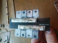
With vertically placed FETs the legs are a ~1mm even shorter, so the inductance is even lower, that matches the tests on my older design, where the inductance was 16..17nH. On that board there was no space for the snubbers, so I made the newer one.
The older board with vertical FETs:

The conclusion is that the vertical placement is significantly better than the horizontal with the legs bent in 90degrees, because the loop inductance is 4-5nH smaller, and also the gate circuit connection is closer to the chip, so the inductive voltages in the gate driver circuit are smaller.
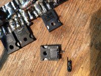
But I wanted to follow the standard procedure, because bending the wide part of the legs is not recommended by the FET manufacturers, so I removed these FETs and changed to IRFP4568-s, because the overshoot was predictably above 100V at 90V supply voltage.
Another option for horizontal placement would be to bend the wide part of the legs in an arc with radius of 1mm, that would be advantageous for both the inductance and the cooling surface, maybe I'll try that sometime on an improved version and I would recommend that for other designs.
The first tests were done with IRFP4110 (100V) FETs, with only 2 of them and the 5 big DCbus capacitors soldered on the board and some small gate driver resistors. The goal of this was to see the high frequency oscillations in the output loop (the 2 FETs and the capacitors) and estimate the loop inductance. It was a double pulse test at 70A on an inductor load that was between the output and the GND, so the high-side FET controlled the transition.
Setup:
This measurement was done with a long probe wire (~40cm) which had some boost at high frequency, and di/dt also induced voltage in the probe loop at the clips, so the amplitude on the waveforms are not exact, but the oscillations are not probe ringing. (I'll post also probe oscillations for comparison.)
These are some typical waveforms with IRFP4110, the first transition on the left is the FET turn-off at the high current, the other on the right is the turn-on.
High side Vgs, marked some points for reference that can be identified on all Vgs and Vds waveforms.
Is: source current of the FET
Irr: reverse recovery current of the other FET
Iout: output current (~70A)
Note that the measured external Vgs is the sum of the internal Vgs on the silicon chip inside the case and the voltage on the source inductance from the chip to outside the case, and ringing at the Miller-plateau of rising edge is on the source inductance (that is a part of the output loop inductance), only a small part of it can be on the chip.
High side Vds:
Low side Vds. The main oscillation appearing everywhere is on the Coss of this FET with the loop inductance after the reverse recovery of its internal diode.
The measured frequency at 60V supply voltage is 42MHz (from number of cycles in 500ns), and the Coss of IRFP4110 at 60V is ~0.6nF (from the graphs in the datasheet), so the calculated loop inductance is 23.9nH, that was better than expected with only the electrolytic capacitors.
Then I added one ceramic capacitor:
High-side Vds with ceramic capacitor:
A little less overshoot and the frequency increased to 45MHz, L reduced to 20.8nH, that is not very much difference.
At the high level a slight ~1.2MHz oscillation appeared, that is a DCbus voltage ringing between the electrolytic and the ceramic capacitors. This must be counted for at high current if there is some distance between different capacitors.
Then I tried one more pair of FETs in another channel with its legs bent at the wide part in 45degrees, because I wanted to test how much the length of the legs change the inductance. The legs are 2mm shorter.
The waveform is very similar so I don't attach, but the frequency increased to 49MHz, and the inductance was 17.6nH. There are 4 legs in an output loop, the difference is altogether 8mm -> (20.8nH-17.6nH)/8mm=0.4nH/mm
With vertically placed FETs the legs are a ~1mm even shorter, so the inductance is even lower, that matches the tests on my older design, where the inductance was 16..17nH. On that board there was no space for the snubbers, so I made the newer one.
The older board with vertical FETs:
The conclusion is that the vertical placement is significantly better than the horizontal with the legs bent in 90degrees, because the loop inductance is 4-5nH smaller, and also the gate circuit connection is closer to the chip, so the inductive voltages in the gate driver circuit are smaller.
But I wanted to follow the standard procedure, because bending the wide part of the legs is not recommended by the FET manufacturers, so I removed these FETs and changed to IRFP4568-s, because the overshoot was predictably above 100V at 90V supply voltage.
Another option for horizontal placement would be to bend the wide part of the legs in an arc with radius of 1mm, that would be advantageous for both the inductance and the cooling surface, maybe I'll try that sometime on an improved version and I would recommend that for other designs.
Probe tuning
Sometimes the oscillation of the probe and the switching circuits can be confused, because they may have similar natural frequencies, mainly if the differential probe is used with a wire extension without damping. So the probe must be checked. The single-ended oscilloscope probes are normally made of lossy cables with internal damping, those are normally good.
I use my own diy differential probe usually with a 40cm long twisted pair with small Hirschmann test clips, but it has some artifacts because its frequency response is not flat, so it is not good for high frequency signals. The wire is an undamped LC circuit.
The probe clips:

The step response of the probe is checked on the output of an LM5163, because at light load it has a fast falling edge without ringing. The rising edge is not so fast, there is no overshoot. The vertical resolution is 16.5V/div, the undershoot is 23V, and there is some HF oscillation:

The rising edge is verified with the probe touched to a DC voltage, and in one out of several trials there is no bouncing, just a single edge with the artifact. I can't tell the frequency, because my diy scope samples at 160MHz, and it's probably above 80MHz, but it is clearly a wire artifact that should be eliminated:

The same wire without the clips is a little better:

With a similar 20cm twisted wire the overshoot is just a small spike:

After many tests finally I made a 11cm long wire with the clips and 100ohm damping resistors between the clip and the wire, that produce no spikes, but does not limit the bandwidth in the range of my scope. The resistors are under the heat shrink:

There is some slow overshoot and undershoot that seems to be high-pass filtering by the amplifier in my diff probe (the frequency compensated divider works in a longer time range), but it's not a big problem, I kept it as it is:


The following tests were done with this probe.
Sometimes the oscillation of the probe and the switching circuits can be confused, because they may have similar natural frequencies, mainly if the differential probe is used with a wire extension without damping. So the probe must be checked. The single-ended oscilloscope probes are normally made of lossy cables with internal damping, those are normally good.
I use my own diy differential probe usually with a 40cm long twisted pair with small Hirschmann test clips, but it has some artifacts because its frequency response is not flat, so it is not good for high frequency signals. The wire is an undamped LC circuit.
The probe clips:
The step response of the probe is checked on the output of an LM5163, because at light load it has a fast falling edge without ringing. The rising edge is not so fast, there is no overshoot. The vertical resolution is 16.5V/div, the undershoot is 23V, and there is some HF oscillation:
The rising edge is verified with the probe touched to a DC voltage, and in one out of several trials there is no bouncing, just a single edge with the artifact. I can't tell the frequency, because my diy scope samples at 160MHz, and it's probably above 80MHz, but it is clearly a wire artifact that should be eliminated:
The same wire without the clips is a little better:
With a similar 20cm twisted wire the overshoot is just a small spike:
After many tests finally I made a 11cm long wire with the clips and 100ohm damping resistors between the clip and the wire, that produce no spikes, but does not limit the bandwidth in the range of my scope. The resistors are under the heat shrink:
There is some slow overshoot and undershoot that seems to be high-pass filtering by the amplifier in my diff probe (the frequency compensated divider works in a longer time range), but it's not a big problem, I kept it as it is:
The following tests were done with this probe.
mxlemming
100 kW
- Joined
- Jul 17, 2020
- Messages
- 1,122
Is it just me that thinks the ESC is a minor achievement compared to the fact that Peters seems to have made his own oscilloscope?
I just bought myself a new scope, looking forward to exciting results. Peters' tip with the 100 ohm resistors will probably work just as well on my scope.
You think the lm5163 is producing perfect square edges? I found some ringing on my old rubbish scope with that chip.
What's the scope software? I presume your board uses some awesome analog devices chip and some fancy opamps with a well thought through layout? The software is the hardest bit. I might have a crack at the scope bit one day.
if you want to mount fets horizontaly you can do it as me in my old controller. THT fets will have always problems with ringing, because they have long legs, and only one bond wire inside them. Better are SMD fets, they have more source legs - can be driven kelvin source, or better some packages have no legs (QFN etc.), Or use new GaN fets 
Attachments
Yes.mxlemming said:Is it just me that thinks the ESC is a minor achievement compared to the fact that Peters seems to have made his own oscilloscope?
A high power motor drive is a bigger challenge.My scope displays the raw samples without fancy digital processing that makes it much more simple than normal oscilloscopes, but the advantage is I can see the real data from the ADC.
The 100ohm works for me with the short wire as on the photo, but with longer wire it forms a low pass filter. But good oscilloscope probes are already damped.I just bought myself a new scope, looking forward to exciting results. Peters' tip with the 100 ohm resistors will probably work just as well on my scope.
Ok, maybe that was probe ringing, too? Could a long GND loop produce that?You think the lm5163 is producing perfect square edges? I found some ringing on my old rubbish scope with that chip.
I tried also with just a few cm short wire without damping, too, the waveform with that was the same as with my damped wire.
Made in VHDL, the sources are shared here if someone is interested:What's the scope software? I presume your board uses some awesome analog devices chip and some fancy opamps with a well thought through layout? The software is the hardest bit. I might have a crack at the scope bit one day.
https://opencores.org/projects/xilinx_scope
Sure, I have some test boards with SMD FETs, too.stepus said:if you want to mount fets horizontaly you can do it as me in my old controller. THT fets will have always problems with ringing, because they have long legs, and only one bond wire inside them. Better are SMD fets, they have more source legs - can be driven kelvin source, or better some packages have no legs (QFN etc.), Or use new GaN fets
But TO-247 with the bent legs are compatible with the normal manufacturing process and there are some other similar ongoing projects on the forum, so I show my waveforms also for reference to see what to expect from such design, what problems can arise and how I handled them.
I have a bunch of more waveforms to present, will post (some of) them today.
mxlemming
100 kW
- Joined
- Jul 17, 2020
- Messages
- 1,122
Peters,
After hijacking your thread to have an argument with Zombiess, I will try to be useful - below are some waveforms for an LM5017 and an LM5163, taken with my shiny new Siglent SDS1104X-E. It's no 1GHz R&S, but general consensus is it is pretty good, and has no trouble resolving up to about 150MHz (3dB point at 140MHz IIRC from various Youtubes, and it carries on resolving up to 200MHz).
My layout is pretty similar to your board, the critical things being to have a ground plane underneath it, and a decent ceramic cap very close to the inputs. I had to use the 10x mode, the bandwidth seems greatly improved that way.
The parts are lightly loaded - both the MCUs on the boards are running, and the total draw is about 1W, most of which is going through the 5V rail.
How I probed LM5163:

The rising edge:

The falling edge:

LM5017 I use on another board. I swapped to this chip because JLC had them, but did not have the LM5163. They are now out of stock of either, because in many ways JLC suck. The 5017 and the 5163 are broadly identical, same use case, almost pinin compatible (I actually swapped them out with minimal hackery).
Probing LM5017:

LM5017 rising edge:

LM5017 falling edge:

Using the ground clip for comparison:

Ringing observed:

I basically did this because I was concerned about the complete lack of ringing/features... started to suspect the scope was doing some kind of digital filtering crappery, but it seems it is not.
Anyways, hope this is useful to you as a comparison of a near identical part and layout.
Compared to my old borrowed from work scope (I gave that back when I resigned a few weeks ago) the ringing is much lower, and the resolved features more detailed. The added bandwidth and 4x the sampling rate are a nice improvement.Probes also seem better
After hijacking your thread to have an argument with Zombiess, I will try to be useful - below are some waveforms for an LM5017 and an LM5163, taken with my shiny new Siglent SDS1104X-E. It's no 1GHz R&S, but general consensus is it is pretty good, and has no trouble resolving up to about 150MHz (3dB point at 140MHz IIRC from various Youtubes, and it carries on resolving up to 200MHz).
My layout is pretty similar to your board, the critical things being to have a ground plane underneath it, and a decent ceramic cap very close to the inputs. I had to use the 10x mode, the bandwidth seems greatly improved that way.
The parts are lightly loaded - both the MCUs on the boards are running, and the total draw is about 1W, most of which is going through the 5V rail.
How I probed LM5163:
The rising edge:
The falling edge:
LM5017 I use on another board. I swapped to this chip because JLC had them, but did not have the LM5163. They are now out of stock of either, because in many ways JLC suck. The 5017 and the 5163 are broadly identical, same use case, almost pin
in compatible (I actually swapped them out with minimal hackery).Probing LM5017:
LM5017 rising edge:
LM5017 falling edge:
Using the ground clip for comparison:
Ringing observed:
I basically did this because I was concerned about the complete lack of ringing/features... started to suspect the scope was doing some kind of digital filtering crappery, but it seems it is not.
Anyways, hope this is useful to you as a comparison of a near identical part and layout.
Compared to my old borrowed from work scope (I gave that back when I resigned a few weeks ago) the ringing is much lower, and the resolved features more detailed. The added bandwidth and 4x the sampling rate are a nice improvement.Probes also seem better
Very useful, thank you very much!mxlemming said:Anyways, hope this is useful to you as a comparison of a near identical part and layout.
I also had a board with LM5017 that induced oscillation on my long probe wire after the rising edge at a certain load current, from which I suspected that had a faster rising edge than falling, and your waveforms prove that, too.
zombiess
10 MW
Peters, you did a nice job working with only 2 layers. My first design was only 2 layers and with parallel devices it was a mess to figure out. Did it take you more than one try?
It is my second of this kind (3 boards stacked, 12-FET with the same main components), the first one was with the vertically placed FETs, but I made several other test boards with only one half bridge.zombiess said:Did it take you more than one try?
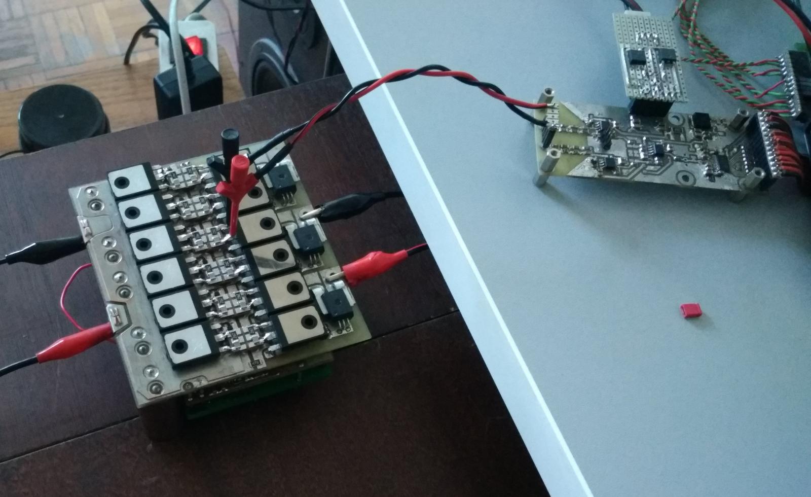
I made several double pulse tests with the fully equipped boards in different configurations at 85V and 210A (105A/FET). This may be interesting for hardcore controller developers only, more or less similar waveforms can be expected with other designs with through-hole FETs.
The tests were made with a ~15uH inductor connected between 2 outputs, and the first 40us pulse raised the current above 210A. The crocodile clips may have some contact resistance (and the wire as well), but this config worked at the current I wanted from the first try, so didn't replace it with a better connector:

The test setup again, the probe clips are perpendicular to the legs of the FET that prevents the di/dt from inducing voltage in the probe that would change the amplitude of the measured signals:
All waveforms were taken at the same timebase, the first transition on the left of the pictures is always the turn-off at the high current, then the turn-on of the second pulse on the right, and sometimes the last turn-off is on the right of the screen.
Test 1.
The first tests are without snubbers and without the external Cgs (C21, C22, etc. on the schematics).
The load inductor is connected between the output being tested and another output at low level, so the high-side FET controls the transition.
The Vds voltages are always in 16.5V/div, the Vgs and others are in 3.3V/div, this is set on my diff probe. The offset of my probe is not centered, so the GND mark on the left of the screen is not exactly at the low level of the signal. The low level is the 0V.
High side Vgs (3.3V/div):

As the common mode rejection of the probe is not infinite, the high side Vgs measurement is always repeated with reverse polarity, and the real signal is the average of normal and the inverted waveforms. For ease of comparison, the picture of the inverted waveform is vertically mirrored:

Common mode voltage on the high side gate:

The di/dt is measured with a 10mm diameter wire loop placed close to the S-D pins of the FET, it works as a transformer:

The di/dt is visible on all other waveforms, too, mainly on the Vgs, because the voltage on the source inductance is superposed on the internal Vgs (on the silicon chip), but this is the pure di/dt:

High side Vds (16.5V/div). The overshoot is ~21V at this turn-off speed. This can be reduced, but then the current turn-off lasts longer that would increase the switching loss:

Low side Vgs. The amplitude of the oscillation after the diode reverse recovery is ~3V, but most of that is just oscillation on the source inductance, there is no shoot-through. The snubber will clean that off. The large negative glitches may stress some weaker gate driver chips (not the ones on my board) and cause latch-up. Perhaps it is the problem with the 3-phase TI DRV-s:

Low side Vds. The frequency of the oscillation after the rising edge is 41MHz, the calculated loop inductance is 19..20nH:

The tests were made with a ~15uH inductor connected between 2 outputs, and the first 40us pulse raised the current above 210A. The crocodile clips may have some contact resistance (and the wire as well), but this config worked at the current I wanted from the first try, so didn't replace it with a better connector:
The test setup again, the probe clips are perpendicular to the legs of the FET that prevents the di/dt from inducing voltage in the probe that would change the amplitude of the measured signals:
All waveforms were taken at the same timebase, the first transition on the left of the pictures is always the turn-off at the high current, then the turn-on of the second pulse on the right, and sometimes the last turn-off is on the right of the screen.
Test 1.
The first tests are without snubbers and without the external Cgs (C21, C22, etc. on the schematics).
The load inductor is connected between the output being tested and another output at low level, so the high-side FET controls the transition.
The Vds voltages are always in 16.5V/div, the Vgs and others are in 3.3V/div, this is set on my diff probe. The offset of my probe is not centered, so the GND mark on the left of the screen is not exactly at the low level of the signal. The low level is the 0V.
High side Vgs (3.3V/div):
As the common mode rejection of the probe is not infinite, the high side Vgs measurement is always repeated with reverse polarity, and the real signal is the average of normal and the inverted waveforms. For ease of comparison, the picture of the inverted waveform is vertically mirrored:
Common mode voltage on the high side gate:
The di/dt is measured with a 10mm diameter wire loop placed close to the S-D pins of the FET, it works as a transformer:
The di/dt is visible on all other waveforms, too, mainly on the Vgs, because the voltage on the source inductance is superposed on the internal Vgs (on the silicon chip), but this is the pure di/dt:
High side Vds (16.5V/div). The overshoot is ~21V at this turn-off speed. This can be reduced, but then the current turn-off lasts longer that would increase the switching loss:
Low side Vgs. The amplitude of the oscillation after the diode reverse recovery is ~3V, but most of that is just oscillation on the source inductance, there is no shoot-through. The snubber will clean that off. The large negative glitches may stress some weaker gate driver chips (not the ones on my board) and cause latch-up. Perhaps it is the problem with the 3-phase TI DRV-s:
Low side Vds. The frequency of the oscillation after the rising edge is 41MHz, the calculated loop inductance is 19..20nH:
Test 2.
Also without snubbers and Cgs, but the load is connected between the output and another output at high level, so the low-side FET drives the transition. Also 85V and 210A.
Low side Vgs. The interesting part is the end of the falling edge that gets to 0V just slowly. It is because the low side FET source is not in Kelvin connection and a part of the DCbus waving voltage between the different capacitors is there at high current. I was thinking on this when I made the PCB drawing, but I wanted to try it. Conclusion is that 10mm distance on a solid plane is inductance. This small fluctuation does not make any problem here and at 100A this effect is hardly noticable, but the Kelvin connection is better in any case:

Low side Vds:

DCbus fluctuation on the ceramic capacitors. The overvoltage is 4-5V that must be taken into account for the supply voltage margin for the capacitors, and at regen braking the voltage will be even higher:

High side Vgs:

High side Vgs with inverted polarity and vertically mirrored. The real signal is the average of this and the normal polarity waveform:

Common mode voltage on the high side gate:

High side Vds:

di/dt at the S-D legs:

Also without snubbers and Cgs, but the load is connected between the output and another output at high level, so the low-side FET drives the transition. Also 85V and 210A.
Low side Vgs. The interesting part is the end of the falling edge that gets to 0V just slowly. It is because the low side FET source is not in Kelvin connection and a part of the DCbus waving voltage between the different capacitors is there at high current. I was thinking on this when I made the PCB drawing, but I wanted to try it. Conclusion is that 10mm distance on a solid plane is inductance. This small fluctuation does not make any problem here and at 100A this effect is hardly noticable, but the Kelvin connection is better in any case:
Low side Vds:
DCbus fluctuation on the ceramic capacitors. The overvoltage is 4-5V that must be taken into account for the supply voltage margin for the capacitors, and at regen braking the voltage will be even higher:
High side Vgs:
High side Vgs with inverted polarity and vertically mirrored. The real signal is the average of this and the normal polarity waveform:
Common mode voltage on the high side gate:
High side Vds:
di/dt at the S-D legs:
Test 3.
High side drive with snubbers, without Cgs, 85V, 210A
High side Vgs. The signals are cleaned from the oscillations by the snubber:

High side Vgs with inverted polarity and mirrored:

High side gate common mode voltage

High side Vds. The overshoot is higher (25V), that is the side effect of the snubbers.

Low side Vgs. Without ringing the signal is better visible and after the reverse recovery it is only +1V, no need to worry about parasitic turn-on. At the turn-off transient (on the left) the positive glitch is higher, but then the Vds of this FET is 0V.

Low side Vds without ringing:

High side FET di/dt:

Low side FET di/dt (in reverse recovery). With snubbers the high and low side current transitions are not exactly the same:

High side drive with snubbers, without Cgs, 85V, 210A
High side Vgs. The signals are cleaned from the oscillations by the snubber:
High side Vgs with inverted polarity and mirrored:
High side gate common mode voltage
High side Vds. The overshoot is higher (25V), that is the side effect of the snubbers.
Low side Vgs. Without ringing the signal is better visible and after the reverse recovery it is only +1V, no need to worry about parasitic turn-on. At the turn-off transient (on the left) the positive glitch is higher, but then the Vds of this FET is 0V.
Low side Vds without ringing:
High side FET di/dt:
Low side FET di/dt (in reverse recovery). With snubbers the high and low side current transitions are not exactly the same:
Test 4.
Low side drive with snubbers, without Cgs. 85V, 210A
Low side Vgs:

Low side Vds:

DCbus fluctuation at the ceramic capacitors:

High side Vgs:

High side Vgs with inverted polarity and mirrored:

Common mode voltage on high side gate:

High side Vds:

High side Vds on the FET parallel with the previous one. The spike at the rising edge is because of the different reverse recovery times of the parallel FETs, and in some cases this can be an overshoot even with snubbers. IRFP4568 on this board has very high reverse recovery charge, other FETs with lower Qrr and Irr are probably better for parallelling:

High side FET di/dt (in reverse recovery):

Low side FET di/dt (driving):

Low side drive with snubbers, without Cgs. 85V, 210A
Low side Vgs:
Low side Vds:
DCbus fluctuation at the ceramic capacitors:
High side Vgs:
High side Vgs with inverted polarity and mirrored:
Common mode voltage on high side gate:
High side Vds:
High side Vds on the FET parallel with the previous one. The spike at the rising edge is because of the different reverse recovery times of the parallel FETs, and in some cases this can be an overshoot even with snubbers. IRFP4568 on this board has very high reverse recovery charge, other FETs with lower Qrr and Irr are probably better for parallelling:
High side FET di/dt (in reverse recovery):
Low side FET di/dt (driving):
Test 5.
High side drive with snubbers and Cgs=3.3nF (C21, C22,...) with 3.3ohm serial resistors. 85V, 210A
The RC circuit between the source and the gate is a negative feedback from the lower end of the source inductance and slows down di/dt if reduced overshoot or smaller Vgs negative glitches are needed.
High side Vgs:

High side Vgs inverted and mirrored:

Common mode voltage on high side gate:

High side Vds:

Low side Vgs:

Low side Vds. The overshoot is caused by the slower stabilization of the driver FET current from Iout+Irr to Iout:

High side FET di/dt (driving):

Low side FET di/dt (in reverse recovery):

High side drive with snubbers and Cgs=3.3nF (C21, C22,...) with 3.3ohm serial resistors. 85V, 210A
The RC circuit between the source and the gate is a negative feedback from the lower end of the source inductance and slows down di/dt if reduced overshoot or smaller Vgs negative glitches are needed.
High side Vgs:
High side Vgs inverted and mirrored:
Common mode voltage on high side gate:
High side Vds:
Low side Vgs:
Low side Vds. The overshoot is caused by the slower stabilization of the driver FET current from Iout+Irr to Iout:
High side FET di/dt (driving):
Low side FET di/dt (in reverse recovery):
Test 6.
Low side drive with snubbers and Cgs=3.3nF with 3.3.ohm serial resistors. 85V, 210A
Low side Vgs:

Low side Vds:

High side Vgs:

High side Vgs inverted and mirrored:

Common mode voltage on the high side gate:

High side Vds:

High side FET di/dt (in reverse recovery):

Low side FET di/dt (driving):

That's all for now.
Low side drive with snubbers and Cgs=3.3nF with 3.3.ohm serial resistors. 85V, 210A
Low side Vgs:
Low side Vds:
High side Vgs:
High side Vgs inverted and mirrored:
Common mode voltage on the high side gate:
High side Vds:
High side FET di/dt (in reverse recovery):
Low side FET di/dt (driving):
That's all for now.
mxlemming
100 kW
- Joined
- Jul 17, 2020
- Messages
- 1,122
I've read this a few times now, and each time it's made sense but the question still in my mind is...
What's the conclusion? Is this fine? You happy with it?
I see a lot of artifacts even after snubbers that I don't get on my later boards and wouldn't know what to make of if i did.
The ultimate test I guess is whether it spins a motor, whether it breaks while spinning and the heat generated.
I'm also wondering about the cause of the "ringing". Is this really resonance on the inductance un the circuit out a kind of fast positive feedback through the miller capacitance causing the MOSFET to rapidly switch on and off as it rises?
I'd really like to see this board built with different FETs that have a lower gate-drain to gate-source capacitance ratio. Like the ones used by Thor in his build.
Yes it's fine and I will put this on my bike after I finish the firmware (that will take some time). I didn't find other complete double pulse test waveforms on the internet when I started to work on controllers, and it was also hard for me to figure out how these should look like. Now these waveforms may be useful as references for others for designs with TH FETs.
But I would improve a few things on the PCB if I ever make a next version, I already mentioned some of them:
1. bend the wide part of the legs of the FETs to the board, that would reduce the inductance and the overshoot by 20..25%
2. place the snubbers on the power PCB instead of the small boards
3. Kelvin connection also on the low side
4. I would consider removing the ceramic capacitors from the DCbus if not necessary to reduce the overshoot
5. replace the FETs with better ones with lower Rdson and reverse recovery charge, either 100V or 150V
To my mind there is big a difference between something works and something is good, and the difference is hidden in the details. Spinning the motor is just the minimum requirement to work (it surely spins, I already tried). The high current waveforms show more information, for example the Vgs and Vds never exceed the limits in the datasheet, the FET doesn't go into avalanche breakdown, optimal dead-time and others. Many parameters depends on the temperature so normally these would be verified at the extreme operating temperatures. If all is ok then it can be expected to be reliable.
Your ~zero inductance design with the SMD FETs and the internal Eddy current shielding is another concept that can certainly switch faster and with smaller transients. I'm also wondering how your waveforms would look like at 100A, the di/dt with a wire loop and others. Maybe it's not so easy to measure the real signal even with the GND sping on the probe, because that is also a loop above a high di/dt zone. Now I'm not sure if I measured properly the SMD FET test boards I made earlier.
I think the ringing is not related to the Miller capacitance. Basically the ringing is between the loop inductance and the Coss of the FET that is in off state after its rising Vds ("07 low Vds IMG_20210303_192703.jpg" above). It rings also at lower supply voltage, but at lower frequency because then the Coss is higher.
If you look at "05 high Vds IMG_20210303_192440.jpg", that is the FET turning on, the oscillation is at the end of the falling edge and after. Most of that ~6..8Vpp oscillation is on the source inductance, there is much less on the silicon chip, so there is not much voltage feedback via the Miller cap. But the oscillating current (between e.g. 90 and 110A) probably makes some change on the internal Vds and/or Vgs (around the Miller-plateau), because the FET current and voltages must be consistent in every moment, on a definite point on the MOSFET characteristic curves (Id vs. Vds parameterized by Vgs). This little feedback may change the decay time of the oscillation, but I don't know how much it counts.
If another FETs on the same board wouldn't oscillate, that would be because of different reverse recovery transients, I think, but I haven't tried these new IRF100Pxx and IRF150Pxx series yet. Older TO-247 and TO-220 FETs I tried all oscillated.
mxlemming
100 kW
- Joined
- Jul 17, 2020
- Messages
- 1,122
Very good. I really owe this forum a high current test. 100A for me, half as many FETs i guess.peters said:Yes it's fine and I will put this on my bike after I finish the firmware (that will take some time). I didn't find other complete double pulse test waveforms on the internet when I started to work on controllers, and it was also hard for me to figure out how these should look like. Now these waveforms may be useful as references for others for designs with TH FETs.
I say this with your signals still having a lot of artifacts I'd be uncomfortable with, not to suggest i think these tests are pointless. I think they're very very good tests.To my mind there is big a difference between something works and something is good, and the difference is hidden in the details. Spinning the motor is just the minimum requirement to work (it surely spins, I already tried). The high current waveforms show more information, for example the Vgs and Vds never exceed the limits in the datasheet, the FET doesn't go into avalanche breakdown, optimal dead-time and others. Many parameters depends on the temperature so normally these would be verified at the extreme operating temperatures. If all is ok then it can be expected to be reliable.
Every time i get better probes/scope I find fewer artifacts. I think soldering twisted pairs to the relevant pins might be required, but even then the probing loop is basically the same size as the board loops so will experience di/dt pickup.Your ~zero inductance design with the SMD FETs and the internal Eddy current shielding is another concept that can certainly switch faster and with smaller transients. I'm also wondering how your waveforms would look like at 100A, the di/dt with a wire loop and others. Maybe it's not so easy to measure the real signal even with the GND sping on the probe, because that is also a loop above a high di/dt zone. Now I'm not sure if I measured properly the SMD FET test boards I made earlier.
I say this because I saw identical ringing on a colleagues inrush current limiter that resulted in immediate FET death. It didn't have the slightest possibility of inductive ringing since it was switching over roughly 1ms. It was stark and obvious that this was the cause of the ringing.I think the ringing is not related to the Miller capacitance. Basically the ringing is between the loop inductance and the Coss of the FET that is in off state after its rising Vds ("07 low Vds IMG_20210303_192703.jpg" above). It rings also at lower supply voltage, but at lower frequency because then the Coss is higher.
If you look at "05 high Vds IMG_20210303_192440.jpg", that is the FET turning on, the oscillation is at the end of the falling edge and after. Most of that ~6..8Vpp oscillation is on the source inductance, there is much less on the silicon chip, so there is not much voltage feedback via the Miller cap. But the oscillating current (between e.g. 90 and 110A) probably makes some change on the internal Vds and/or Vgs (around the Miller-plateau), because the FET current and voltages must be consistent in every moment, on a definite point on the MOSFET characteristic curves (Id vs. Vds parameterized by Vgs). This little feedback may change the decay time of the oscillation, but I don't know how much it counts.
If another FETs on the same board wouldn't oscillate, that would be because of different reverse recovery transients, I think, but I haven't tried these new IRF100Pxx and IRF150Pxx series yet. Older TO-247 and TO-220 FETs I tried all oscillated.
With these FETs at this current the artifacts are normal and unavoidable. For example turning off 100A on a 5nH source inductance in 150ns generates 3.3V and it can be seen on the Vgs waveforms. Likewise for turn-on, reverse recovery and on the Vds waveforms.mxlemming said:I say this with your signals still having a lot of artifacts I'd be uncomfortable with, not to suggest i think these tests are pointless.
marcos
1 kW
- Joined
- Nov 19, 2016
- Messages
- 348
There is a detail in your power supplies that got my attention because I used the same part#.
That series zener in series with the lm5164 input is something original, havent seen it before so I had to try it. It didnt work very well for me, but I experienced failures in that supply so it was interesting to see extra care protecting it.
Thanks for sharing peters!
That series zener in series with the lm5164 input is something original, havent seen it before so I had to try it. It didnt work very well for me, but I experienced failures in that supply so it was interesting to see extra care protecting it.
Thanks for sharing peters!
mxlemming
100 kW
- Joined
- Jul 17, 2020
- Messages
- 1,122
marcos said:There is a detail in your power supplies that got my attention because I used the same part#.
That series zener in series with the lm5164 input is something original, havent seen it before so I had to try it. It didnt work very well for me, but I experienced failures in that supply so it was interesting to see extra care protecting it.
Thanks for sharing peters!
Where's this Zener? Isn't peters using lm5163? I can't find this Zener.
I'm intrigued because I experienced a few failures with lm5163. Lm5017 seems much more robust. I have also considered putting a resistor and tvs/Zener on the dcdc input.
Did you also find the 5163 ripple was worse than expected? Even using ti web bench designer i never got close to the specified values with 5163. Lmr36510 and lm5017... All but perfect.
marcos
1 kW
- Joined
- Nov 19, 2016
- Messages
- 348
LM5163 and LM5164 are pretty similar, from what I can see its only different current ratings. Even the LM5017 looks similar to me, why do think its more robust?
Yeah voltage ripple was higher than advertised and even made audible noises so it took me extra time to get it right. Had to use the fancy feedback network and even the output voltage wasn't spot on.
Yeah voltage ripple was higher than advertised and even made audible noises so it took me extra time to get it right. Had to use the fancy feedback network and even the output voltage wasn't spot on.
Similar threads
- Replies
- 182
- Views
- 54,997
- Replies
- 3
- Views
- 2,210
- Replies
- 65
- Views
- 10,679