20Kw motor and 300A ESC (ultralight aircraft propulsion system)

Mihai_F

100 W
Joined
Oct 11, 2021
Messages
161
Hy guys, i will move here the discussion about my 20Kw motor and 300A esc. This is been a project for my past 6 years, it's been a huge learning curve. Before i started this project my experience with electronics was with power audio circuits, analog stuff, and nothing digital.
I will start first with the electronic speed controller because that took most of the time to learn and develop.
So i begun with a BLDC monolithic driver chip, the MC33035, and i made the circuit with wires, it took me a month to get it running and be able top spin a small BLDC sensored motor, it looked like this:
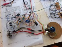
IMG_3111.JPG
It was capable of about 12w ,24v at 0.5A, then i learned what MOSFET stands for: Magically Obliterated, Smoke and Fire Emitting Transistor, i was amazed how much smoke can make a TO220 packge :oops: , inductance was my friend (bundle of wires), but at that time i was blissfully unaware of it. Then i learned a few things and moved the project to PCB, i was so impressed about my first toner transfer technique PCB, but from electrical stand point was crap, again i did not know that, this is how it looked,
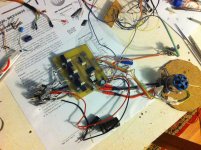
IMG_3139.JPG
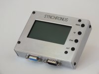
This was the first year and it was capable of about 48w ,24v at 2A, before it wood magically let the smoke out of the FET-s, at that level i learned about that thing called "ringing"... :oops: .Then i learned a lot more things, i added a few functionalities like safestart, rpm, voltage, current and tep readout, all made on 4 digit 7 segment display, it was a lot of work, and it looked like this, (the big motor was made at this point) ,
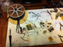
IMG_3577.JPG
This was the second year it was capable of about 120w , 36v at 3.3A, o about that time i realized i need to move up a bit and enter the AVR microcontroller world, i knew nothing about them, and all i knew about C programming language was that there was some things called "if" and "else"... :shock: , then another year of huge learning curve and another variant of the controller came witch was way easier to customize and change things, hence programmable microcontroller, it looked like this
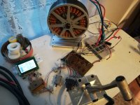
IMG_20190403_195721.jpg
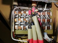
This was in the third year became V1.0 it is capable about 2.5kw 20S(84v) 30A (current sensor limited),IRFP4468 FET-s , it has BMS and a lot of functionalities including 128x64 GLCD with menu where a lot of parameters can be customized, then the learning curve was the most steep making the ESC to work up to 16kw, then i learned what inductance can really do, and what miller plateou, reverse transfer capacitance, stray inductance, and a lot of goodies that give a lot of headakes.... :shock: , then came next variantwitch looked like this
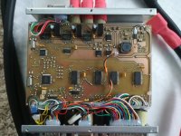
IMG_20191126_150448.jpg
IMG_20200325_010057.jpg
testout2.png
This was in the fifth year, v1.2 witch worked up to 16Kw at 20S (84V), IRFP4468 FET-s (6/plase), PCB-s made by me. It was the first and last time i tested the motor by holding the table just myself... :shock: :lol: :lol: , it was exiting seeing my work succeed, but kinda scary because i could barely hold the table, the prop was pulling 78kgf :shock:
https://www.youtube.com/watch?v=NTU_feiQHvM&t=4s
This was how later tests were made, the motor was strapped by the car, no more worries about flying with the table
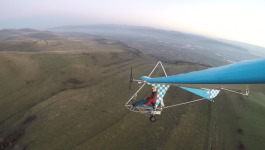
Zb SyGoat p2.png
This was in the 6-th year the flight testing.
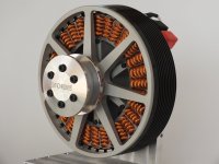
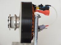
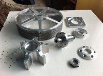
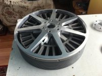
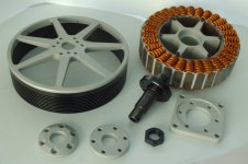
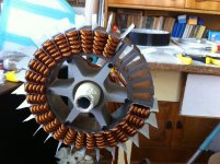
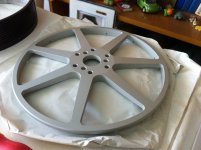
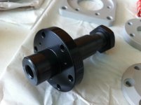
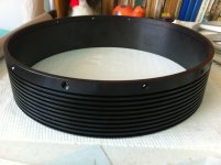
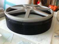
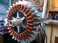
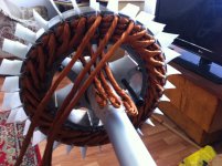
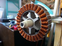
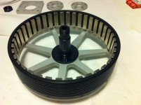
The motor was made by scaling up a smaller motor, (was still 20pp and 30 teeth but only 10kw), i did calculations for the winding, i drew it in 2D cad, went to a machine shop and told them what parts i need, the stator laminations were laser cut (unfortunatly 0,5mm thick), then a full day of winding. It was not even by far such complex to make as the ESC.
It's mass is 7.7kg, 216mm OD, 40mm stator hight, 40x10x5 N45 magnets, 6mohm and 10uH per phase, delta terminated, 3 halls and 1 temp sensors. It can do 16Kw continuous and 22Kw max (1 min) at 20 deg C ambient, being air cooled ambient temp affects max power.
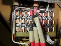
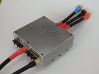
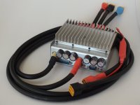
And here are some photos of the system.
DSCF6975.JPG
DSCF7024.JPG
DSCF6985.JPG
DSCF7008.JPG
DSCF7006.JPG
IMG_3385.JPG
IMG_3384.JPG
DSCF7237.jpg
IMG_3400.JPG
IMG_3401.JPG
IMG_3402.JPG
IMG_3405.JPG
IMG_3406.JPG
IMG_3418.JPG
IMG_3420.JPG
IMG_3422.JPG
IMG_3464.JPG
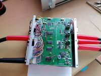
And in the present the 7-th year V1.3 (IRF150P220 FET-s) gives headakes as mention in my other post (300A ESC help...). The change (FET-s) was made in order to go with 22s battery.
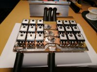
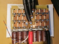
It looks like this, with PCB-s made by specialized company, power board has 1mm thick water jet cut busbars.
IMG_20210226_110552.jpg
IMG_20201219_124842.jpg
IMG_20210106_143647.jpg
This is just a short story, the hole experience has waaaaaay more detalis and waaaay more headakes.
There is a lots of room for improvement, this is very low tech, and to some may be even foolish, i know, up to this point it was the best i could do, but will see what future shows up.
 
Huge respect for your amazing efforts and accomplishments! Wow!!

What a huge evolution and progression! Congratulations on flying your own controller and motor!
 
Shiver me stator plates lad!! That is one fine motor! If you built that motor the first time through, then it's got to be
a first,.. no prototypes? No suffrage? Totally in awe. :shock:

The six screws holding the laminations in place have me a bit freaked, but must be a time tested method, and if it
jerks, it works, so I guess it's all good.

Lost me after the first photo on the controller,.. you have a real knack for electronics and that was certainly a massive
effort, but your doggedness paid off. :thumb:

Your workmanship is impeccable!, and I'm still trying to find my jaw... dropped it om the floor somewhere...
 
Thank you guys for your appreciation !

APL said:
... If you built that motor the first time through, then it's got to be
a first,.. no prototypes? No suffrage? Totally in awe. :shock:
...Your workmanship is impeccable!,...

Well the build quality it is mostly because of the CNC machining, my job is CNC mill machinist, so this just standard practice to me, even if the parts were not made at the shop where i work (various reasons), i knew exactly how to draw it, what to put and how to put it where it needs to be, so that i get best results.
This is probably why i see some very awesome ESC around here, the people that made them work with electronics or they studied in collage electronics. My education nor my work never included electronics, i learned electronics from internet as a hobby, and this is why my electronics have a noob hobby look like :oops: :D

This is the first try and first motor built (the prototype), there are a few twiks here and there to be made on the next versions (if any) and the only thing that i assumed it might be needed to be redone is the winding, and there was no need because it came out good (parameters are ok, Kv ) mostly because i had a careful look at how others did it (no. of turns) in order to learn and did my own calculations to see how will it be. I'm sure that it can be adjusted (the winding and the stator) for even better results to refine the efficiency, but for now it does a pretty good job, i mean it took my ass in the air, and it stayed just worm and not in :flame: :flame: . :mrgreen:

The controller electronics on the other hand, they need some more work, probably even more than i know at this state of knowledge, but i'm getting there slowly......sadly not enough time, life gets you...

As a side note the plane was also built and tested by me from 2013 till 2020, since then it became my life style and what i am wight now, a TON of learning, but where there is will there is a way!
 
Like the back story. Going from machinist to power electronics is quite a sidestep. Not too many transferable skills so well done... Getting code to run even block commutation on avr is tricky enough (I've done this and eventually moved to stm32 after pressure from colleague) so double well done for getting basic programming skills. What's your toolchain for firmware? Arduino or atmel studio?

My day job is mech eng, which I dare say I'm very good at, but that means for my home projects I do *the bare minimum possible* to make the mechanical aspects tangible. I have virtually zero interest in mechanical engineering outside work... Maybe I should dust off the solidworks on my personal laptop and send some drawings out for my motor to just get it right and perfect first time rather than messing with 3d prints on parts sketched up in half an hour...

Have you discovered the joys of kicad yet? If not, you should. It doesn't take long to learn if you're halfway good at mechanical CAD and I can point you towards some good starting layouts for power stages. If you learn the basics of GitHub you could push the designs to the web and I can poke them for you. If you got your power stage into kicad and made it a 4 layer board with overlapping ground and+ I think you could quickly make big changes to the inductance situation and order jlcpcbs for all of a few euros.
 
The toolchain is atmelstudio. The software that i use for pcb is Copperconnection from Robotroom, 6 years ago was free, but then was bought by a big company and now it does not exist anymore (officially) .... :shock: I will give a try to kicad, i heard of it but never used it.
As for a 4 layer power board, i am affraid that the traces and gnd an v+ will be to thin for 300A, unless they can laminate 0.5 to 1mm thick coper in it, i had a try with thin traces and they kinda vaporized.
It is a delicate problem to solve, it can be solved with 6 ot 8 layer board, having 2 gnd, 2 v+ and 2 sw node thinner plains (0.25mm) to spread the current, but that smells expensive.
I had bashed my head around a lot on how to make a high current board and not be crazy expensive, and be doable with the technology that i have around.
One thing that i will like to try, is use igbt power modules with laminated bus bars (gnd and v+) and move away from TO247 packges, but i think that will not be as compact anymore, and is way more expensive, i checked a few possibilities but they are 600v rated, a bit overkill for my application , hence the pryce.
As of now power bord is 148 x 98mm, with 18 fet-s, i made it as small as possible, to be as compact as possible, but not having parallel gnd and v+ plains, creates a lot of loop area, from the ringing that i have (6Mhz) and the Coss of the fet-s it calculates an inductance of about 75nH, witch is 10nH +10nH fet legs + 30nH sw node (60x20mm trace) and + 25nH power traces (70x50mm). As others users here made power boards with TO247 they reduced inductance down to about 12nH and still got ringing but at higher Mhz, i guess that for our designs we are stuck with snubbers to tame the ringing....
 
Mihai,

A while ago, because I spent a lot of time reviewing other power stages on here (there was a bit of a spat of them earlier this year) I went and laid out what I thought at the time was probably a fairly optimal layout.

https://endless-sphere.com/forums/viewtopic.php?f=30&t=111585

The files for it are on Github
https://github.com/davidmolony/MESC_MODULAR/tree/master/MESC_18_FET_THROUGH/MESC_18_FET_THROUGH

It received relatively little interest, but you might consider looking at it to solve your inductance situation - I think this design achieves 3 things:
1) The only inductance of any significance it that caused by the MOSFET and shunt resistor packages themselves
2) The recirculation currents during the PWM low take short paths, and those paths are on the top surface where it is trivial to reinforce with large lumps of copper.
3) The returns for the gates and switch nodes are optimised for low inductance and low coupling to the power rails.

The size was 50x100 for TO220 FETs, so the size for TO247 fets would increase I think by an extra 9*5.8mm = 52mm, 152mm total, which is not much more than your board. For your application, you could easily mod it to have a single shunt resistor, or whatever topology you are using and lose the low side/phase shunts - significant simplification.

Or just take a look and take any learnings you want :)

KiCAD, and the layout is absolutely free to take and use as you want. Just install KiCAD, download the project folder and open it. I never ordered any of it not because I didn't think it would work or I wasn't happy with it, just... 1) my main job turned insanely busy and 2) I can't buy the micros to run it at the moment anyway so what's the point.

If you go for the big IGBT packages, you will hit other serious problems - the package inductance situation is far more complex, you will need much more complex gate driving circuitry, and they switch REEEEAAAALLLLYYY slowly. You'd be looking at a BoM cost 5x what your current one is and a lot of extra headaches. But you could rewind your motor and run at 400V and far less current.
 
mxlemming said:
Mihai,

A while ago, because I spent a lot of time reviewing other power stages on here (there was a bit of a spat of them earlier this year) I went and laid out what I thought at the time was probably a fairly optimal layout.

https://endless-sphere.com/forums/viewtopic.php?f=30&t=111585

The files for it are on Github
https://github.com/davidmolony/MESC_MODULAR/tree/master/MESC_18_FET_THROUGH/MESC_18_FET_THROUGH

It received relatively little interest, but you might consider looking at it to solve your inductance situation - I think this design achieves 3 things:
1) The only inductance of any significance it that caused by the MOSFET and shunt resistor packages themselves
2) The recirculation currents during the PWM low take short paths, and those paths are on the top surface where it is trivial to reinforce with large lumps of copper.
3) The returns for the gates and switch nodes are optimised for low inductance and low coupling to the power rails.

The size was 50x100 for TO220 FETs, so the size for TO247 fets would increase I think by an extra 9*5.8mm = 52mm, 152mm total, which is not much more than your board. For your application, you could easily mod it to have a single shunt resistor, or whatever topology you are using and lose the low side/phase shunts - significant simplification.

I took a look at you design, i got inspired and learned from it, and started designing a new powerboard (v1.4 :D ).
On the v1.3 power board i went with 22r on gates and 20n+1.8r snubbers, that cleaned the ringing and weird pulses on t-on/t-off at no load, but sadly with increasing load the "bad things" start to appear again, few at light load, and more at greater loads, it turns out, as you pointed out, these faster fet-s need fast and low inductance design, the slower fet-s on v1.2 did not had such headaches, but the huge inductance every where on v1.3 bites back hard, i get all possible ringing scenarios that i could read about (toshiba app notes suggested by some guys here).
It is frustrating after all that work i thought v1.3 wood be better than v1.2, but it is worst and it does not work, this is a huge step back, but learned hard lessons. I have to take a few days off from working on it, so the frustration calms down :cry: , then i'l get back at it :D . Dang it, my perseverence is some times shaded by stubbornness, but i guess they go hand in hand.... :p
 
Good luck with it! I do worry occasionally that those FETs might be all but unusable being so fast but with such high package inductance. Still, if you use something similar to my layout on 4 layer board your board inductance should be down to single digit nH, plus 20ish for the package...

The key could be in the ground and switch returns as much as the main loop inductance.

If you ever re do the driver board and still have issues you might want to use the gate drivers zombies does... Td350e or something. They have a staged turn off mechanism for active Miller clamping.
 
Just came to show my appreciation. What an incredible project. Its beautiful craftmanship. Well done!
 
Thank you everyone for you appreciation!

I had a look at power board v1.2 and compared it to v1.3, and made a list with differences and similarities, then i remembered (a year ago i woked on it) what made v1.2 functional, and v1.3 does not have, and these are: 6 x 0.1uF ceramics and 15 x 1uF ceramics between + and- bus bars (earlier v1.2 had pp caps, the red ones, but worked with those to), and external Cgs caps on low side fets (4468 needed external Cgs to reduce ringing at turn on), without those v1.2 did not work. So somewere somehow i decided that v1.3 does not need them, because busbars made from one piece each and better/faster fet-s :roll: :shock: :oops: ....
I will add those, and give one more try to v1.3.

(this is the link https://endless-sphere.com/forums/viewtopic.php?f=30&t=113704 describing the problems of v1,3)

I red a some topics here with THT fets ringing
https://endless-sphere.com/forums/viewtopic.php?f=30&t=55641&start=150
https://endless-sphere.com/forums/viewtopic.php?f=30&t=49450
https://endless-sphere.com/forums/viewtopic.php?f=30&t=91689&start=200
https://endless-sphere.com/forums/viewtopic.php?f=7&t=97699&start=125
and a few more,

And i have a few questions:
1. on a 18 fet-s power board when adding snubbers all fets must heve them, or one snubber on each half bridge (3fets) or only on low side fet-s (the ones that cause problems) . Note i have PWM only on low side, NO synchronous switching, 6 step block commutation.

2. adding external Cgs cap, that improves Cgd/Cgs ratio, and slows down switching/ reduces ringing, but does it help on keeping the Vgs level (low or high) more sturdy ?

3. how do you connect the Gnd from gate drivers (ir2110s) to the Source of the fet-s (power board Gnd)?, how not make a ground loop , right now all 3 gate drivers have Gnd connected together and it goes to the Lm7812 then to the Lm517 buck and the thru supply wires (8cm twisted +and- HV) to the power board Gnd at the - bat cable, and i think that is no good (v1.2 worked that way somehow... :roll: ) if i connect each gate driver to the respective fet-s, how do i connect them to the regulator Gnd?
I know i will get a lot of criticism about that... :mrgreen:

4. what benefits are if PWM is on low side or high side or both (NOT talking about synchronous switching, i know that has benefits)

these might be noob questions but i want to get those wright, from the "experts"

IMG_20200325_010057.jpg
IMG_20201125_154022.jpg
 
Hi Mihai,

I'm certainly not feeling like I have enough experience to be an "expert" but I think I can answer your questions correctly :D

1) You need 1 snubber per phase, i.e. per group of MOSFETs ASSUMING the link between the paralleled MOS is low inductance. The snubber circuit inductance needs to be low compared to the MOS circuit inductance otherwise it is going to struggle to snub the ones further away.
2) Extra Cgs helps stabilise the Vgs, again, assuming it is placed close to the leg of the FET and the inductance between the gate and the external cap is small. If it is not, you can create ringing and oscillations between them. You probably do not need it if your FETs are good Cgs to Cgd ratio, but it's worth fitting the footprint. Marcos, Zombies, Peters told me this a year ago and I have been doing it since.
3) The PGND of the driver (also labelled COM I think?) should ONLY be connected to the FET source, by a wire or small dedicated plane parallel and close to the gate line. The VSS of the gate driver, that is signal ground, should be connected to your ground plane and the other gate drivers and the ground of the regulator, switchmode DCDC etc. This is covered in various appnotes, and you will see it observed on the layout I made.
4) You should normally have the low side FETs conducting and PWM the high side on. This limits the time the bootstrap capacitor is being used to turn on the FETs and maximises the time it is charging. This is especially important at low speeds and startup.

At low and intermediate speeds, using low side as usually on does stress the low side FETs more (as high side usually on would stress the high side ones more), which is one advantage of sinusoidal control, but you're not going that way so irrelevant...

Regarding the ceramics on the power line, I consider these essential. They should be as close to the FETs as possible, since the voltage bounce the switch node will see is determined by the inductance of the entire changing loop, not just the FETs. The loop continues all the way back to the decoupling capacitors. The value of said caps should be sufficient to absorb about half the current for the duration it takes for the electrolytic's to get into action. Say 500ns switching 300A and accepting 5V bounce you'd want something like 15uF of ceramics minimum. I would be inclined to have more since they don't cost that much.

I have a board where I can switch 300A in <100ns with very little overshoot and practically no ringing. Heat is a different problem, it cannot do this for long (like only a few seconds...). It uses TOLL FETs, and has very low inductance. I have about 30uF of ceramics spread around the FETs, with 2400uF of electrolytics nearby. This is more ceramics than I need for sure, but they were 0.02$ per uF on JLCPCB so I just went for loads of them.

As your switching period gets longer, the ability of your electrolytics to absorb this requirement increases.
 
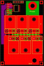
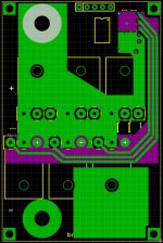
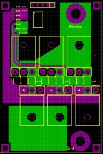
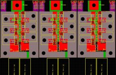
I have been working on the new power board design V1.4 , 4 layer, it is work in progress, not finished yet, and if you can give some opinions on layout of the gates and switching loop.

I got inspired from mxlemming (most of it), zombies (on board per phase) and a bit of peters(fet-s staggered), designs:
https://endless-sphere.com/forums/viewtopic.php?f=30&t=111585
https://endless-sphere.com/forums/viewtopic.php?f=30&t=58341
https://endless-sphere.com/forums/viewtopic.php?f=30&t=110674&hilit=Peters+controller

So it goes like this;
top are V+ and Gnd,
inner upper is Gnd shield,
inner lower are Ls gate driver Gnd, and Hs gates,
bottom are phase, Ls gates, and Hs gate driver Vs,
Al high current traces/planes on top and bottom will be 1mm thick copper wather jet/laser cut like V1.3.

I tryed to keep the switching loop area small and also being able to put ceramic caps between Fet-s V+and Gnd, bus plates will be a bit narrower (only to the midle of the fet-s legs holes) so that ceramic caps to NOT solder directy on them (i ain't gonna make that mistake twice :flame: :flame: ) , the Dc link caps will be on the side of the board like V1.2 and V1.3, still have to figure out how and where i connect V+ and current sensor, this time i want to use bolted lugs instead of soldering the cables on the bus plates, the gate driver chip is in there because i wanted to see is fi can fit it there, also give some opinions if is best to put gate drivers on same board with power stuff, or on separate board, i still have to decide if to use the same gate driver IR2110, witch worked great in the past,or to migrate to more fancy driver like TD350E.
After rearranging the fet-s, a wider heat sink was needed (200mm) so I decided to do 3 separate boards (98x65mm), mainly because cost, JLC pcb rips off, if board is 195mm wide, plus i had a lot of trouble soldering / reflow the bus plates on the pcb and not have the board warping out of shape, so having 3 smaller boards with a bit of space between them might be easier to install the bus plates.

Here are the layouts:
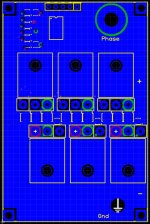
pb-v1.4-top.jpg
pb-v1.4-bottom + inner lower.jpg
pb-v1.4-inner lower + bottom.jpg
pb-v1.4-inner upper.jpg

Edit: i fixed a mistake on gate traces connection to Ls fet-s (was conected to S not to G)
 
This is generally how I would aim to do it if i played with through hole FETs.

However, your copying zombiess multi board approach probably necessitates copying his use of isolation as well.

There are simpler isolated gate drivers than the ones peters and zombies use, ucc21520 for example, but availability might be tricky now and you lose the desaturation protection.

No snubbers so far but lots of room for them. Give yourself plenty of snubber capacity.

How come you can't get the width of a single board down to 9x the width of to247fet?
 
mxlemming said:
No snubbers so far but lots of room for them. Give yourself plenty of snubber capacity.

How come you can't get the width of a single board down to 9x the width of to247fet?

yep i'l will put the snubbers i'l have to find a good place for them

I tried a version with 9 fets in a raw on a single board, and was about 166mm, but there was not much space for gate routing without crossing under the high current planes, and i will try to avoid that as much as possible, plus having 2 166x30mm copper bus plates on the length of the board is it very tricky not to warp the board when soldered or reflowed, v1.3 had 3 120x25mm phase plates on the length of the board and i had a tough time installing them wright. And some guys suggested that the thermal cycling on such a board might be a problem (death by 1000 cuts).
Another factor is the available heat sink shape, 100x200 (fins on 100) or 150x200(fins on 200). V1.2 and 1.3 had 100x150(fins on 100), it was just fine there was no need for more. So with fet-s re arranged i have to pick 100x200, the 150x200 is way overkill, plus is 400 grams heavier and that weight sits in the front of the plane, witch changes the CG, not good, so to keep in mind that it has to fly i don't want extra unnecessarly weight. Also the volumetric efficiency of the hole thing is important, i don't want a big draggy brick in front of the plane, i have done a few rearrangements and a few sketches to see how different and big it gets, so far with the 100x200 sink i get the lowest profile and weight increase.
 
mxlemming said:
No snubbers so far but lots of room for them. Give yourself plenty of snubber capacity.

are you refetring to V+ to Gnd snubbers or D-S fet snubbers?
V+ to Gnd snubber (decoupling) caps are there 9 ceramic pieces between the V+ and Gnd plains, per board, they will be 6x1uF and 3x10uF ceramics, i made foot print larger for 10uF it is 2220smd .

the D-S fet snubbers might place them on the bottom layer

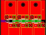
pb-v1.4- supply ceramic caps.jpg
 
Drain source rc snubbers I'm referring to; switch node to ground.

I see your Vbat to ground caps, good placement. Looks like plenty.

I encourage you to reconsider the seperate board thing. The ground and VDC links are part of the switching loop. They're decoupled by the ceramics and the electrolytic caps but every pwm cycle you're still switching the full 300A between them.

This is where isolation and laminated busbars become a necessity. You might get away with it if you put the boards right next to each other and link them with short wires/plates...

Something I tried a while ago was putting bends into the 0.5mm copper I reinforced a PCB with which allows it to flex with differential expansion/contraction. You don't need to solder it down all the way along the PCB like you often see, only where the current needs to enter and exit. The pcb planes will take the high frequency stuff.
 
I have changed the layout a bit in order to better acomodate the battery feed to the boards, i added snubbers they are over the fets close to the legs to keep inductance small, added foot prints for external Cgs, gate pull down resistor and TVS (or zenner), the gate traces are routed outwards and away from power traces and with gnd plane under them + plus the shield (blue plane).
The battery cables will be connected (bolted) to the middle board and from there to the left and right boards on top and bottom with busplates (not shown) will feed those boards, another idea might be to use the heatsink for transfer of the B- from the center board, since the heasink must be grounded, bolt to the heatsink each board B- . Each board has its own 2 dc link caps, but the load is shared across all 6 .
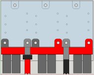
On the top of the boards the grey power traces are the 1mm copper bus plates, they are not all the way to the middle, so that ceramic caps (10 x 4,7uF in the midle ) are stress free. The bottom phase power trace will be 2 x 1mm thick plates to handle the current since they are so narrow, will have about 18sqmm.
I'm committed to 3 separate boards, one for each phase, in the future they will have on top each its own driver board (work in progress)
If you guys have any suggestions or see some obvious layout rule violations please point it out.
here it goes:
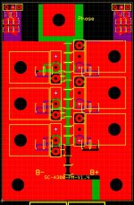
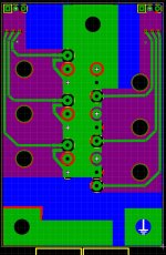
pb-v1.4.1-top.jpg
pb-v1.4.1-bottom + inners.jpg
pb-v1.4.1- 3boards+top bus plates.jpg
 
hey guys,the power boards are on they'r way to europe (jlcpcb), in the meantime i'v been redesigning all the power distribution section and the casing, most of the work and taught was for the laminated busbars, i have found this https://www.youtube.com/watch?v=zGsHuoK9Egs they give some good hints there,
this is so far but still needs some attention after seeing that video.
black and red are B+ and B- cables, black rectangle over B+ is current sensor, dc link caps are in pairs of 2, distributed over the length of the bus bars.
any hints are well appreciated.
sc-a300-v1.4-busbars.jpg
 
Mihai,

Each power section looks good on it's own but by splitting the boards I'm basically outside my level of experience.

If you connect the boards together with a low inductance link, laminated busbar like you are targeting, it should behave like a single board again.

Did you split the blue ground plane?
 
spinningmagnets said:
What is the kV of the motor? Thanks for posting this wonderful project here!

Kv is 36, delta terminated. 10x for appreciation.
 
Back
Top