Gate driver design with TD350E

Okey. I read your post concerning desat calculation.
https://endless-sphere.com/forums/viewtopic.php?f=30&t=61937&p=940576&hilit=desaturation#p940576
As the current which goes from td350e desat pin is 250uA I see that it is curcial to read voltage from zener diode datasheet when conducts this amount of current. From datasheet this small amount of current could not be read.
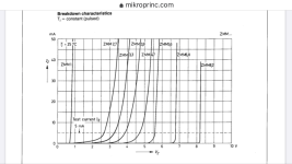
CE353E4A-9716-4C2B-84D1-C32A70522CFB.png
If I choose to order new diode it will take a long time before it comes. Maybe I could use one allready available. I have diodes with 5.1v 5.6V and 6.2V.
I can place on of them 5.6V in desat circuit and measure voltage across it with scope. Fet will work with some average current level. Will this be good result concerning diode voltage at 250uA current?
 
I have found i usually end up with a zener around 5.1V for MOSFETs between 5-10mOhm. I suggest you start with a higher value though. This way desat triggers at a lower current so you can become more familiar with it.

When you do order parts, order an assortment. I keep a selection of low value 2512 gate resistors and various zener values on hand so i can tune various gate drives.
 
Yes I will do that on next ordering.
Desat test was done high fet GS short and coil between low fet and +.
Concerning desat seems that diode (5.6V) which I had showed ok for now. I measured with scope voltage across it and it looks like voltage on it is 5.6V.
Voltage across zener 5.6V diode
CBA19602-F042-485E-AF35-3DD056ABE030.jpeg
I run couple of tests here are results.
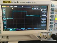
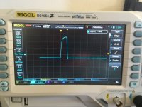
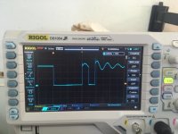
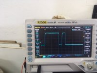
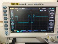
Voltage pulse from mcu 300uS long.
439C9084-CDE8-4DE6-8D95-772D9666C432.jpeg
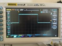
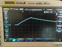
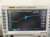
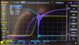
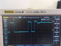
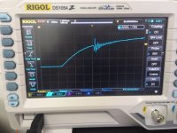
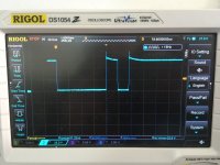
Voltage pulse at desat pin about 175uS.
Maximum point reached is 7.2V
D12B59D9-8534-46AC-8292-C9173BF85879.jpeg
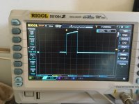
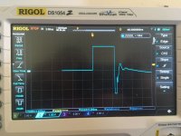
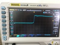
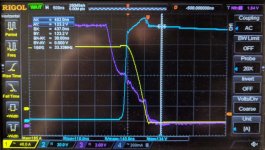
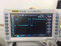
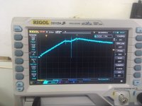
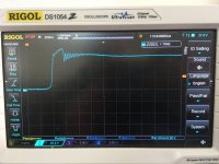
Voltage at fault output pulse about 175uS.
I think that on picture is seen fault state from previous test and reseted with new pulse and then again low because desat triggered.
0A1CD2C1-73AD-4C0D-A37B-DCAFCE922CAE.jpeg
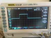
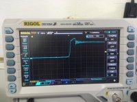
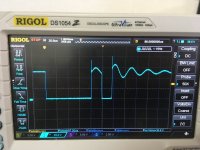
Current through coil is about 110A peak and reached in 175uS. Measured with 10mR shunt.
C10D4164-72FA-455D-BED8-35BEAA4BC391.jpeg
Currently don’t have Vgs shoot but it is also about 175uS.
By some calculations and shoots above seems that desat triggers at 7.2V, zener diode voltage is 5.6V, current * Rdson_irfp4668( 110A * 0.008R) .
7.2v = 5.6v + 0.88v + Vdiode
=> that Vdiode is about 0.72V
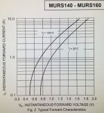
Diode is murs160-13-f.
Looking at forward characteristics and taking into consideration measurement erros and parameters variation it could be this forward drop respect to small current from TD350.
96672646-3130-4FCD-A459-FED336D09DF0.jpeg
 
Tested with short instead coil. Same configuration hi fet GS short and just current sense resistor 10mR between low fet D and + power supply. Pulse from mcu was 300uS.
Vgs low fet.
9938BB82-9B8B-45EA-8F21-5CF0F3F77F05.jpeg
Voltage on 10mR shunt.
A23624E5-43FB-4848-8F98-C71A7CA6E774.jpeg
Current reached about 260A and protection triggerd in about 4uS. Power supply was 60V and with 260A gives significant amount of resistance just with shunt installed. Think that solder joints influence a lot since didn’t have right tool for copper sheet soldering.
 
I always enjoy watching desat do it's job, i just don't like to see it trigger in use. I've had it save my controllers during tuning, especially when the controller loses sync at high current. It just takes time to go through and test different fault conditions and dial everything in.
 
Yes very interesting. I will see how it works first with H bridge, then test with 3 phase.
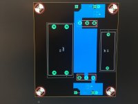
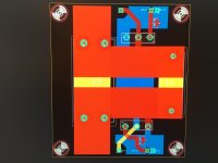
In meantime worked on power stage. Here are some pics. Send to manufacture and waiting for the boards. Did with 4 layers as original design.
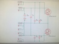
Schematic
022A475F-4331-40AB-8B49-9C7070D5D7C4.jpeg
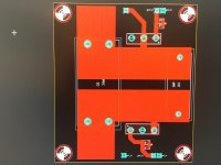
Top
E8FFC9E8-EFDE-453B-874F-5B6083FEFD36.jpeg
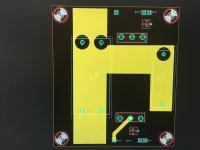
Layer 2
893DD8D9-EBB4-46DF-A703-EB8FF328B5C8.jpeg
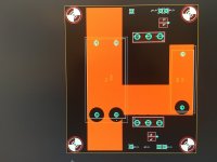
Layer 3
3A88E1CF-9453-4FA7-85F7-A3B0903D9A02.jpeg
Bottom
D6F05FF4-EA6B-4631-B4BD-E48ED724CF56.jpeg
Complete board
BB823A78-F32E-458C-9B07-1AAC7958794B.jpeg
Mask is removed from bottom and top for soldering copper sheets. For dc link cap used 30uF polyprop EZP-E50306MTA.
 
PCB should work as it previously worked for me. My new designs use a better layout, but i have not shared them. I've moved to 6 layer PCBs and can obtain low inductance <20nH. That PCB was a compromise to allow installation of 12mm x 6mm copper bussing in a side by side config. It supported +100A DC.
 
I hope so :) For this older design did you specify custom core, prepreg, thickness and distance between layers? I couldn’t find this information from board in KiCad. Also this depends of manufacturer. I am using JLCPCB but they have only two options for 4 layers boards and offering some inductance calculator. Asked them but they could not provide explanation so I went with default option. Based on your experience how much of peak power this configuration of board can handle concerning its inductance? Lets say that other factors are not limiting it like caps, fets, gate drivers and power tracks current handling capability.
If I want to rework this board into 6 layers what would be your recommendation concerning layer arrangement?
I have just recieved differential probe so soon I will test and post results.
 
bdj said:
I hope so :) For this older design did you specify custom core, prepreg, thickness and distance between layers? I couldn’t find this information from board in KiCad. Also this depends of manufacturer. I am using JLCPCB but they have only two options for 4 layers boards and offering some inductance calculator. Asked them but they could not provide explanation so I went with default option. Based on your experience how much of peak power this configuration of board can handle concerning its inductance? Lets say that other factors are not limiting it like caps, fets, gate drivers and power tracks current handling capability.
If I want to rework this board into 6 layers what would be your recommendation concerning layer arrangement?
I have just recieved differential probe so soon I will test and post results.

https://www.youtube.com/watch?v=E_la_VfrjTM

I did short 18-20kW peaks on my ebike with 30s with something like 300a phase.
 
Very nice!! You used RS232 for communication with Labview at what speed? Did you had any issues with communication concerning noise from switching? And what about added caps polyprop or electrolytics?
 
bdj said:
Very nice!! You used RS232 for communication with Labview at what speed? Did you had any issues with communication concerning noise from switching? And what about added caps polyprop or electrolytics?

Labview setup was something Joby Aviation had for controller testing and that the other guy in the video had setup. I just brought a controller to test. It was a very fun and interesting learning experience.
 
So I can't help wondering why the convoluted bus shape of the inner layers.
Why, for example, is the bat- in the second yellow layer not underneath the read bat- on the upper layer?
 
Think this is question for zombiess as I just followed close his own design. Beside things which can be found among posts I don’t know much about requirements of power stage pcb design. I could just guess that induction would be lot more having two - or two + layers one next to other. In case of + and - layers fileds would be opposite direction so resultant induction would be lower.
 
The way I understand it and I'm no high power engineer, is that inductance is built up in the wire (just like impedance). Having a layer below does affect it but I've never seen a mention of current direction being a factor. I would think crosstalk would be more of an issue.

Also I was thinking the current goes out one phase and come back in a different one, so not underneath.

I also came across a potential nice alternative for the TD350E.
with all the bell and whistle : infineon EiceDRIVER™ 1ED38x0Mc12M or simpler one 1ED3122MU12H
 
squeegee said:
So I can't help wondering why the convoluted bus shape of the inner layers.
Why, for example, is the bat- in the second yellow layer not underneath the read bat- on the upper layer?

It's an old design and not laid out in an optimal way.
 
squeegee said:
I also came across a potential nice alternative for the TD350E.
with all the bell and whistle : infineon EiceDRIVER™ 1ED38x0Mc12M or simpler one 1ED3122MU12H
Looks nice I will order and try this simpler one. Take a look also on STGAP2S from st. I allready make a pcbs and plan is to test it as soon as finish testing with power stage.
Zombiess can you give some info in short how this older design could be reworked?
I tested diff probe from micsig DP10013. Repeated double pulse test so here are results.
Results from using regular probe could be found on earliar posts in this topic.
Second rise egde of Vgs of lower fet.
D2CEDE43-D961-46C8-8775-A9859448E14A.jpeg
Vds of lower fet.
1E74606A-70F0-4E20-A613-0FDEA55FAC25.jpeg
 
bdj said:
squeegee said:
I also came across a potential nice alternative for the TD350E.
with all the bell and whistle : infineon EiceDRIVER™ 1ED38x0Mc12M or simpler one 1ED3122MU12H
Looks nice I will order and try this simpler one. Take a look also on STGAP2S from st. I allready make a pcbs and plan is to test it as soon as finish testing with power stage.
Zombiess can you give some info in short how this older design could be reworked?
I tested diff probe from micsig DP10013. Repeated double pulse test so here are results.
Results from using regular probe could be found on earliar posts in this topic.
Second rise egde of Vgs of lower fet.
D2CEDE43-D961-46C8-8775-A9859448E14A.jpeg
Vds of lower fet.
1E74606A-70F0-4E20-A613-0FDEA55FAC25.jpeg

How much current was in that pulse? Looks OK to me, it can be difficult to reduce the turn on noise into current as it's literally a shoot through event, just very brief.

To improve on that old design I'm not sure what I'd do as I've changed strategies. It works but could be improved upon as the copper bus bars are pretty far apart, so they don't as much canceling effect of the EMF. What matters is if it works for you. When starting out one of the best things you can do is replicate a known result. Makes troubleshooting much easier.

Here are some scope shots from a double pulse test I just did on two parallel IRFP4568's. 400A at 120V DC bus for comparison. Has a 22nF G-S resistor, 15ohm on 7.5ohm off, TD350E gate drive, 25uH load coil and DC bus is <20nH. Desat is set to kick in at 550-600A.

Voltage measurements were done with differential probes and current was measured on the source leg with a Rogowski coil.

2x_irfp4568_400A_on.jpg
2x_irfp4568_400A_off.jpg
 
It was about 50-60A. Probes could be even better connected. Currently couldn’t manage to connect them to be at exactly where legs leave package but plan is to test again. Doing measurements I see that every part of mm on a fet legs means a lot concerning quality of results and get a sense if could measure with probes couple more mm inside package that turn-on noise would be even lower.
zombiess said:
When starting out one of the best things you can do is replicate a known result. Makes troubleshooting much easier.
Agree.
Very very clean result especially for current measurement. Bandwidth of your Rogowski coil is 10MHz?
I will soon test same thing with my cheap Rogowski coil from aliexpress.It is big and conductor is thick so I must free some space between fet legs. Leg could not be in centar of conductor as it has huge diameter so some nonlinearity should occur. I will post results.
 
My Rogowaki setup is from Athena Energy who appears to now be out of business. The probes i have can . measure up to 220A and have a bandwidth of 30MHz. They also cost about $1k usd and I have two for doing parallel device research. Totally worth it imo, but I'm obsessed with high current and parallelization.
 
I saw some of their models on ebay but could not find any info. I tested coil from aliexpress seems that can not hit bandwidth near 100KHz but in specification says that can easily go to 10MHz and factory confirmed :D.
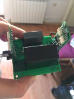
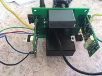
Boards arrived and one phase is assembled here are some pictures.
sl1.jpeg
sl2.jpeg

I did double pulse test again. Everything is same(coil, gs resistors, gs caps, duration of pulses..) as tested earlier only power supply for low fet is +15V and -5V and removed 2200uF from dc link as used earlier on setup.

Here is Vds of low fet (only PP cap 30uF + small one 2.2uF also PP).
image0.jpeg

Same thing but added 47uF electrolytic cap in parallel.
image1.jpeg

Added 2200uF electrolytic cap in parallel.
image2.jpeg

Vds zoomed.
image5.jpeg

Vgs from current setup (when added 2200uF).
image3.jpeg

Vgs second rising edge.
image4.jpeg

Current through coil (250mV equals 25A).
image6.jpeg

All measurements are done with diff probe.
Seems that 30uF + 2.2uF is small as there are lot oscillations on Vds or small esr of these caps could be a problem as oscillations are not damped fast enought? Caps from power supply are about 30000uF and wires are long less than 20cm and connected to + and - of power stage.
 
What does it looks like when you remover the 2.2uF? I've seen additional caps cause oscillation as they can form another LC tank circuit.
 
Here is pic when removed 2.2uF.
D54EC084-1EFE-4AFB-9576-B6B95245897F.jpeg

Graph looks almost same if I try adding 0.1uF PP.

Here is added 330uF electrolytic (330uF + 30uF PP).
E0C4B079-8205-4AA9-8E16-287B9CBDFB1C.jpeg

Then removed all caps. Install only electrolytic 330uF and poliester wima 1uF . Here are results.
130528C0-7AB8-4447-8526-7244EA81706D.jpeg
E9F175D2-7F99-419E-B33F-7A9AF7BA37BA.jpeg
 
I'd use that last setup with just the 330uF as it has the best waveform and try to improve the layout on the next revision now.
 
Ok plan is assemble second phase, connect them and test H-bridge with real load.
When assembling second phase I will experiment with different gate resistors(SMD) to extend fet switching time and maybe this Vds oscillation with PP caps would be smaller.
Concerning testing what would be good practice?
Did you test every gate driver on desat and double pulse in yours 3-phase bridges designs?
Did you test desat by turning both phase fets to on at same time or 3 phase connected short and turning on diagonal fets same time?
Any good guide, manual, best practices concerning layout?
 
bdj said:
When assembling second phase I will experiment with different gate resistors(SMD) to extend fet switching time and maybe this Vds oscillation with PP caps would be smaller.

I have not seen the low frequency oscillation change much by altering switching speed as it's mainly tied to the DC bus inductance and the DC link caps. With enough capacitance added the frequency can be made lower, but you will still be introducing additional frequency harmonics into your load.

Concerning testing what would be good practice?
what do you mean?

Did you test every gate driver on desat and double pulse in yours 3-phase bridges designs?
On the first build I like to test everything. A bad solder joint (curse lead free solder) can make a heck of a difference. I recommend testing everything so you have a known starting point.

Did you test desat by turning both phase fets to on at same time or 3 phase connected short and turning on diagonal fets same time?
I test desat by replacing the load coil with around 25cm of wire and doing a double pulse into it while monitoring the current drawn from the pulse caps. I have a LEM 600A sensor which works great, has around +/- 2000A range and costs $25 USD.

If you want to see what a desat looks like without pulsing it, just desolder one of the diodes connecting to the TD350 on the desat pin and it will force it to trigger.

Any good guide, manual, best practices concerning layout?
I've read many tips and tricks in application notes and thesis papers. I can't recall seeing a good guide. If you search for SMPS and loop area you'll start finding papers that will have tips. Simulating through SPICE is super helpful to understand where noise is coming from and what changes to make to stop it.
 
Back
Top