Gate driver design with TD350E

zombiess said:
With enough capacitance added the frequency can be made lower, but you will still be introducing additional frequency harmonics into your load.
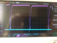
Yes but wouldn’t high inductance motors “eat” these harmonics so they will not reflect current and torque. Currently am buliding this for motors having from 1mH to 2.5mH. So current controller would not have to fight with such disturbances. I see that problem coiuld be with low inductance motors. Anyway I plan to redesing power stage but what inductance of power stage is good to supress these low freq oscillations? In earlier power stage(two copper sheets and capton tape between) it was measured about 20nH and in some point I tested with only PP caps and still there was low freq oscillations.
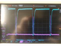
I saw couple of commercial products of dc drivers for cnc machines they use combination of higher value of electrolytic capacitor with low value of PP or poliester cap. Could the issue of low freq oscillations in my case be from transformer power supply(and its caps and internal inductance)? I am thinking that batteries you used for your testing acting like “perfect” power source compare to my power supply with transformer, rectifier and electrolytic caps.
zombiess said:
what do you mean?
You answerd.
 
I made some measurements in meantime.
f0 = 30.49MHz
when added 32nF
f1 = 5.49MHz
Calculated that pcb inductance is 25.4 nH.

I was testing and tried different combinations of GS caps, Ron and Roff values.
At the end used on both fets Ron = 20R, Roff = 10R and GS caps of 55nF.

For a test setup setup used a coil ~70uH connected between common node and + .
Fets were triggered using complementary PWM.
Duty cycle was set to have about 40A in average on coil.

Here are some shoots.

Low fet Vds turn off (yellow Vds, blue DC link, purple is difference (high fet turn on))
2.jpg

High fet Vds turn off (yellow low fet Vds, blue DC link, purple is difference(high fet Vds turn off))
1.jpg

Concerning shoots Vds voltage is measured with regular probe and DC link voltage with diff probe. Also high fet Vds voltage was measured with diff probe and results are same. Diff probe was earlier tested with both end short on common node while switching and scope showed very low voltage - about 2V I think.

I am concerned here with high fet Vds oscillation and it's peak. With this setup overshoot is 50% reaching its peak in 90V. If I put 33nF instead 55nF on GS of both fets this oscillation is even bigger it goes up to 150V. Zombiess from your measurements on first and second controller I see that you deal a lot with double pulse and low fet Vds and setting GS cap according to overshoot on low fet Vds.
But what about high fet Vds overshoot and how did you handled?
Do you have shoots and can you post here?
Situation is same if coil is placed between common node and - .
Just this huge turn off overshoot could be seen on different fet.
I saw some of your earlier measurements and think that is same scenario from link
https://endless-sphere.com/forums/viewtopic.php?f=30&t=51342&hilit=ZombieSS%27s+power+stage&start=325
Here is shoot
shoots.jpg

There is a nice document from nexperia maybe it is already posted on forum but I couldn't find it.
https://assets.nexperia.com/documents/application-note/AN90011.pdf
 
bdj said:
There is a nice document from nexperia maybe it is already posted on forum but I couldn't find it.
https://assets.nexperia.com/documents/application-note/AN90011.pdf

Here's another one on just the snubbers.
https://assets.nexperia.com/documents/application-note/AN11160.pdf
 
bdj said:
But what about high fet Vds overshoot and how did you handled?
Do you have shoots and can you post here?

All changes were made consistent through the design to keep symmetry. What ever was done to either a high/ low side was also done to the other.

My high side / low side tests always look about the same, unless I made a mistake somewhere which has happened more times than I like to admit :)
 
I have completed H bridge, final configuration is Ron 27R, Roff 10R and GS caps of 55nF. Gate driver power supply is +12V and -5V.
Tested with coil and two different DC motors from 1-2mH inductance with locked rotor scenario. Duty cucle was changed from 0% to 50% and current was from 0- 50A. DC power supplu was 90V in allmost all tests.
A0FB8E6B-8D0F-428B-A1F2-8C6AA4D19DBA.jpeg

I am driving H bridge with bipolar pwm’s about 1uS dead time. One diagonal with gate drivers is connceted pwm and other diahonal is connected to pwm complement. I noticed strange issue when duty cucle was in range from 1% to 10% in both directions.
Here are Vds waveforms of two fets(one bottom and one up).
4F17B0AB-0D3B-45AD-A9FC-07DB830862E8.jpeg
63D0D8E7-81FB-4276-AFF5-978C56AD1C91.jpeg
744F8CB6-8F9E-43B0-81D0-89C902D34D46.jpeg
6A34F25D-5307-42FB-A54D-26E6E39D8FB2.jpeg
After 10% of duty ratio fets Vds looks normal and same up to 50A.
88DD9F33-C85C-4CB6-AA49-5C6AC9C92F11.jpeg
Pictures above are meade with dc motor 1mH and 1.6R . From 1-10% of duty ratio current was measured from 0 - 1 A.
When tested witah air coil 70uH and 0.1R also 1-10% duty, current waseasured from 0-20 A.
Here are waveforms of same fets Vds when driving coil (18Amps).
89453C46-2F32-4897-8C43-38096EAA493D.jpeg
Gate signal looks good and no overlaping. No excessive ringing and no false turn on. Currently TD350E desat pin is connected to ground on all drivers.
916BB8E8-DF4A-4D16-B734-E729ABC3D7C7.jpeg
What could be issue here? Any toughts?
 
When troubleshooting, it's advantageous to monitor the Vgs vs Vds vs Pulse input if possible.

How long does it take to get to at least 8V on Vgs?

If this is happening at low duty cycle, you might be switching too slowly to get the MOSFET into saturation. 27 Ohms coupled with a 55nF G-S resistor seems overkill. I would expect it to be no more than 20 ohms on and maybe 10-20nF on the G-S cap if it's needed.

I have also run into issues on the PWM side where my pull up resistor to the TD350 input was too weak which also caused slow turn on and required substantial dead time. A changed it out to 620 ohms to resolve that issue.

Start at the very beginning and trace your way through the circuit under the problematic conditions, you'll find the culprit.

PWM->Opto->Driver->MOSFET
 
Thanks for fast response.
I did test as you suggested. Rise time of Vgs from -5V to 8V is 3uS. Changed pwm from 0% to 10% in 2-3 steps, Vds slope is changing significantly. Did test on all 4 fets mostly turn on waveforms. Load was dc motor 1.6R and 1 mH locked rotor with current up to 1A.
Light blue is mcu pwm.
Yellow is 6N137 output.
Pink is Vgs measured on fet legs.
Dark blue is Vds.

Upper left fet 2% pwm.
F4D6DE6A-6F75-45A7-B50B-7E1C975FE688.jpeg

5% pwm
D339D2BE-B3B8-4221-9EAE-758C1DDB407B.jpeg

10% pwm
E4299DB2-3C65-4A68-BBD5-5FBF51225ECD.jpeg

Down left fet 2% pwm (only have turn off waveforms)
C4150889-CA72-448A-9816-958AE4E68BD7.jpeg

5% pwm
C80F5631-9EFA-420D-BD8E-04654B45072F.jpeg

Right upper fet 2% pwm
BD1CC058-CB7D-4CE5-84EC-88C285996F15.jpeg

5% pwm
34B66EC9-F687-4BEA-9D9B-4AA6A659295F.jpeg

10% pwm
FB65B57D-0F73-417D-8CD9-5247F04A28A3.jpeg

Down right fet 1% pwm
F87AA38D-853E-455A-9404-0FB62C3BE368.jpeg

2% pwm
157B1469-5B5B-467D-96EE-DDD9B5F46F4A.jpeg

5% pwm
F0FD991C-3146-4FB5-91D7-989EA1D6A5E8.jpeg

10% pwm
D8745720-A6A3-46E1-8DD0-12CB280EBE33.jpeg

After these shoots I removed 27nF from all GS. So left on GS with about 27nF and 27Ron. And do some tests but this time with coil connected instead dc motor. Current on 1-10% dytu was max 10A. Still same issue. Now have a more current also on low dytu cycles and noticed that Vds fall edge broked into fast transition fall edge and one additional pulse.
Vds of some fet.
D587CA51-E851-45F2-BA8B-F57056595D34.jpeg
 
If you have a time take a look of this document.

https://unbscholar.lib.unb.ca/islandora/object/unbscholar%3A9775/datastream/PDF/view

9D242E56-2811-4393-878D-E736BFD4FAC3.png

I think it is not issue of switching fets it could be as described here distortion as combination of dead time(during which diodes will conduct) and operating mode when average inductor current is around zero and changes direction during pwm period.
 
bdj said:
If you have a time take a look of this document.

https://unbscholar.lib.unb.ca/islandora/object/unbscholar%3A9775/datastream/PDF/view

9D242E56-2811-4393-878D-E736BFD4FAC3.png

I think it is not issue of switching fets it could be as described here distortion as combination of dead time(during which diodes will conduct) and operating mode when average inductor current is around zero and changes direction during pwm period.

Page 35 of that PDF shows a nice example of dead time distortion. I only skimmed it, no time to read it right now, but I've modeled some of what they are talking about in the past with Simulink and Spice. Took a lot of brainstorming to figure out how to configure variable dead time / bipolar / unipolar center aligned PWM in simulation.

Something to be aware of is runt pulses which can be caused by too short or too long of a period, dead time plays into this. Make sure to configure your controller software to prevent runt pulses which don't switch the MOSFET on the entire way.
 

Attachments

  • Runt Pulse.jpg
    Runt Pulse.jpg
    101.9 KB · Views: 899
  • No Runt Pluse.jpg
    No Runt Pluse.jpg
    111.5 KB · Views: 899
Is it possible to share some of your sim models :)?
zombiess said:
Something to be aware of is runt pulses which can be caused by too short or too long of a period, dead time plays into this. Make sure to configure your controller software to prevent runt pulses which don't switch the MOSFET on the entire way.
ATTACHMENTS
Yes I read about it among the posts. If this is left unresolved what could be issues? Fet will be in liner mode and heat? Does SOA from datasheet refer to operation limits in this scenario?
 
bdj said:
Is it possible to share some of your sim models :)?

I won't share them, it takes quite a bit of work to learn how to generate these types of signals and that is where the real learning happens. I learned by reading papers similar to the one you posted and replicating the research (start simple).

Yes I read about it among the posts. If this is left unresolved what could be issues? Fet will be in liner mode and heat? Does SOA from datasheet refer to operation limits in this scenario?

The device could be left in the transconductance region, it might not turn on for several pulses causing the inductor to discharge which could cause instability in the control system.

The datasheet isn't very useful for this as it has to be figured out on the bench during tuning. You should look at it as an entire system and try to understand how all of it works, from the physics to the control theory. It's a ton of info to learn, but even just having basic knowledge will improve your design skills.
 
Okey.
I turned on again desaturation detection. Seems that fault pin is floating between 5V(fault pin is connected with resistor to opti diode and then to 5V) and 12V( + power supply of TD350E) but no low level output. Here are waveforms on all 4 fets with probes on fault pin and ground).
These two pictures are fault pins of low side fets.
4BE90483-B886-4B51-8827-377859F24ACB.jpeg
4744D5CA-DAAF-4D3D-8CA5-FD3F52BC8900.jpeg
These pictures are fault pins of high side fets.
ECD619D1-00A2-41B9-91D8-E915D976BD5C.jpeg
37F50B48-6A11-4B92-8305-B90BBD6DD2AE.jpeg
B95EEEFA-AC78-4B92-9402-D1880686332B.jpeg
Could this issue be resolved with pull-up to V+ so fault would be always on defined level? I think that didn’t noticed this earlier while testing desaturation.
 
Looking at original design.
design.JPG
Seems that on high fet gate signal passes above power section common node forming S from high fet and D from low fet. On low fet, gate signal passes above - dc bus. Doing double pulse tests separately on high and low fet I noticed little differences in gate signals concerning noise and differences in Vds (there is 10V differences in overshoot). If I understand right would be better to remove common node under the hi side fet gate and would I get same response concerning noise and overshoot?
I am wondering why is better to overlap common node with DC bus concerning inductance?
There is layout example from STGAP2 driver and I don't see that common node is overlaped with dc bus.
layout.png


In meantime I made gate driver with STGAP2 and tested it with same power stage (IRFP4668). Here are schematic, layout and some shoots from double pulse test. GS caps 27nF, Ron 27R, Roff 10R, gate driver supply (-5V, +10V), current 40A and 65V dc bus. Tested with air coil.
Design followed recommendations from eval board.
https://www.st.com/content/ccc/resource/technical/layouts_and_diagrams/schematic_pack/group0/a5/25/94/36/2f/d9/4a/9a/EVALSTGAP2SCM_SCHEMATICS/files/EVALSTGAP2SCM_SCHEMATICS.pdf/jcr:content/translations/en.EVALSTGAP2SCM_SCHEMATICS.pdf
https://www.st.com/resource/en/datasheet/stgap2s.pdf

Schematic
IMG_7289.JPG
Layout
IMG_7290.JPG
Board
IMG_7291.JPG
Vgs -> blue, current -> yellow
IMG_7278.JPG
Vgs second rising edge
IMG_7279.JPG
Vds of pulsed fet
IMG_7281.JPG
Vds of other fet
IMG_7285.JPG

After these tests I decided to test with different fets and used this one NTH027N65S3F.
https://www.onsemi.cn/pub/Collateral/NTH027N65S3F-D.PDF
Here are some shoots from double pulse test. Test configuration is same.

Vgs -> blue, current -> yellow
IMG_7244.JPG
Vds first rising edge
IMG_7252.JPG
Vds second rising edge
IMG_7257.JPG
Vgs second rising edge
IMG_7258.JPG
Vgs second falling edge
IMG_7259.JPG

What could be a problem here? Is issue in probes ? Different output capacitance of fet matched with layout inductance and form slowly damped oscillations? Bad combination of dc bus caps with fet? Small dc bus voltage (this fet max Vds is 650 V) increases output fet capacitance and thus oscillations?
 
bdj said:
Okey.
I turned on again desaturation detection. Seems that fault pin is floating between 5V(fault pin is connected with resistor to opti diode and then to 5V) and 12V( + power supply of TD350E) but no low level output. Here are waveforms on all 4 fets with probes on fault pin and ground).

Could this issue be resolved with pull-up to V+ so fault would be always on defined level? I think that didn’t noticed this earlier while testing desaturation.

The fault pin does not need a pull up, it's active low, so when there is no fault, it should be reading ~5V.

Did you ever tune the desautration detection circuit?

1. Verify stable power (UVLO will trigger a fault, nice benefit of active low fault)
2. Verify the desat triggering threshold by monitoring the voltage on the desat pin of the IC. A fault should trip when it reaches ~7.2V, but I've seen it trigger as low as 6.9V.
3. Verify you have enough blanking time.
 
bdj said:
Looking at original design.
design.JPG
Seems that on high fet gate signal passes above power section common node forming S from high fet and D from low fet. On low fet, gate signal passes above - dc bus. Doing double pulse tests separately on high and low fet I noticed little differences in gate signals concerning noise and differences in Vds (there is 10V differences in overshoot). If I understand right would be better to remove common node under the hi side fet gate and would I get same response concerning noise and overshoot?
I am wondering why is better to overlap common node with DC bus concerning inductance?

The high side gate trade does not cross into any power section, it is above it's ground reference which is the high side MOSFET source. The ground plane is tied to the ground source using a kelvin type connection. This type of connection is used to minimize noise transfer from the power section to the gate drive section.

Draw out each current loop and you'll see that the gate drive is separate from the power pass. Small loop area is key for noise mitigation.

There is layout example from STGAP2 driver and I don't see that common node is overlapped with dc bus.
layout.png

I'm not clear on what you are talking about.

After these tests I decided to test with different fets and used this one NTH027N65S3F.
https://www.onsemi.cn/pub/Collateral/NTH027N65S3F-D.PDF
Here are some shoots from double pulse test. Test configuration is same.

What could be a problem here? Is issue in probes ? Different output capacitance of fet matched with layout inductance and form slowly damped oscillations? Bad combination of dc bus caps with fet? Small dc bus voltage (this fet max Vds is 650 V) increases output fet capacitance and thus oscillations?

I'm going to PM you on this one. For that voltage range you might have better results with a IGBT.
 
zombiess said:
Did you ever tune the desautration detection circuit?
Yes, some test are on second page of this thread but it seems that I missed something. I didn't verify blanking time and also went with zener diode witch has no specification for such small amount of current 250uA but it seems to work and reaching 7.2V with enough current through fet.
I will investigate this further and get right zener diode.

zombiess said:
it is above it's ground reference which is the high side MOSFET source.
Yes my mistake, that is desirable to be above it's ground reference concerning inductance as I read this somewhere in other posts.

zombiess said:
There is layout example from STGAP2 driver and I don't see that common node is overlapped with dc bus.
layout.png
I'm not clear on what you are talking about.
In original design plane which connects D of one fet and S of other fet (phase) is overlapped with + and - dc bus planes (4 layer pcb) but in stgap2 layout example they used 2 layer pcb and didn't overlapped D-S plane with - dc bus plane nor + dc bus plane. So layouts are done differently. My question is what are pros and cons of both approaches?
 
bdj said:
In original design plane which connects D of one fet and S of other fet (phase) is overlapped with + and - dc bus planes (4 layer pcb) but in stgap2 layout example they used 2 layer pcb and didn't overlapped D-S plane with - dc bus plane nor + dc bus plane. So layouts are done differently. My question is what are pros and cons of both approaches?

Sometimes it just comes down to design choices, what will fit and other design specs you might need to meet. In most of my designs I have the phase output on top of the DC bus using PCB or cut copper sheets. I don't see any issues with this and haven't run into any in my own testing. I have a design where my gate drive is about 10mm above my power pass section which sees +300A peaks and I've pulse tested to +600A while monitoring gate drive and signal traces directly above and haven't seen any noise issues, but I made design choices to help mitigate noise pickup. It's not an ideal placement, but I had very tight packaging constraints.

All my loop areas are small on the power pass and gate drive, so noise transmission and reception is minimized.
 
Hi, it has been a while and I was testing H bridges(one with with STGAP2 and other with TD350E).
I was thinking about some changes of position of gate driver so here is picture.
design.png
Horizontal board is power stage board. Vertical board is gate driver and it is soldered directly on fet legs. Gate loop area would be smaller. Gate driver board would have stiffer mechanical connection in comparison to earlier version(in my case gate driver board was soldered via 3 pins to power stage pcb).As drawback I can see double soldering and desoldering if want to change fet. Care should be taken concerning clearances concerning gate driver and power stage as well as gate driver and heatsink.
What do you think?
Can you recommend me some IGBTs and FETs (suitable for motor drives) if I want to work with higher voltages up to 350V dc and currents(peak) up to 40-50A?

I was thinking about :

fets:

IPW60R024P7
https://www.infineon.com/dgdl/Infineon-IPW60R024P7-DS-v02_00-EN.pdf?fileId=5546d462696dbf120169b48730044ab3

STY145N65M5
https://www.st.com/resource/en/datasheet/sty145n65m5.pdf

STWA75N60M6
https://www.st.com/resource/en/datasheet/stwa75n60m6.pdf

igbts :

STGW60H65DFB
https://www.st.com/resource/en/datasheet/stgwa60h65dfb.pdf

IKW75N60T
https://www.infineon.com/dgdl/Infineon-IKW75N60T-DS-v02_08-EN.pdf?fileId=db3a304412b407950112b42890113e25

IKW50N60DTP
https://www.infineon.com/dgdl/Infineon-IKW50N60DTP-DataSheet-v02_01-EN.pdf?fileId=5546d46253a864fe0153cbc2c1c17cc1
 
You've seen in my design how I mounted the gate drive at a 90 myself, so yeah, I approve. It puts the gate drive at a 90 from power pass EMI.

I have not worked with any devices over 200V, so I don't have any recommendations.
 
Okey, thanks :thumb:
Some of these fets and igbts I already ordered and soon they should arrive.
I will test and share findings.
 
Back
Top