• Howdy! we're looking for donations to finish custom knowledgebase software for this forum. Please see our Funding drive thread

Heavy cargo hauler project

dnmun said:
measure the gate voltage of the charging mosfet and the output mosfets. that will tell you is they are turned on.

i just destroyed a battery by discharging without a BMS, spaced it out and now it is blown up like an accordion. damn, whatta lotta money down the drain.

Aw that sucks dnmun :( hopefully a one-off mishap.

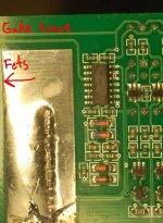
I followed the last paragraph in this post to determine gate voltages. I started in the 'C-' corner worked from left to right, turned around towards the center of the pcb and moved from left to right down the opposite side. Gate voltages are as follows:

Charging FETs
+0.52v
+0.44v
Output Fets
+13.16v
+13.16v
+13.16v
+13.16v

+13.17v
+13.16v
+13.17v
+13.16v
+13.16v
+13.16v

I appreciate your patience with me, thank you. whats next?
-Tom
 
SamTexas said:
Hmm... I assume you have already verified that the charger is functioning and is not the problem. So the only thing left is the BMS. You could try to swap the BMS but that would be a lot of work.

Yup the charger works flawlessly with my other pack so I've crossed that off the list. I have also cut the shrink wrap off the top of the pack and did a continuity check on all wires coming in and out of the pack, between the pack and the bms, and between the bms and external plugs. Everything but the undiagnosed bms seems to check out.

SamTexas said:
Have you tried to bypass the BMS? That is connecting the charger directly to the battery terminal (you don't have to remove the BMS). Do that for 10 mins or so and see if the battery voltage goes up.
I'm quite hesitant with bypassing the bms, as with my luck I'd likely brick the pack. The approach would be to connect the charger directly to the terminals of the pack where the thick output wires connect, yea? I suppose 10 mins cant do much damage, and a meticulous recording of the before-after voltages could shed some additional light on the issues. My charger is current limited to 5.2A. Will this be too much?
-Tom
 
Cargo_Tom said:
I'm quite hesitant with bypassing the bms, as with my luck I'd likely brick the pack. The approach would be to connect the charger directly to the terminals of the pack where the thick output wires connect, yea? I suppose 10 mins cant do much damage, and a meticulous recording of the before-after voltages could shed some additional light on the issues. My charger is current limited to 5.2A. Will this be too much?
-Tom
Only one of two main wires go through the BMS, usually the negative one. You have recently replaced the BMS, right? So you should know which is which. Anyway, if 10 mins is uncomfortable, you can try less. In fact just a few seconds could prove if the battery can take charge or not since you have a voltmeter that can measure to the thousandth volt. 5.2A is definitely not too much. You have a 20Ah pack, right? So that's only 0.26C.
 
I've been having to charge without a Hyperion balance charger or BMS this past 2 weeks. I use Cellogs and have the alarm set for 3.5 for HVC, and D/C at 2.9. I still can get 20 miles out of the pack. New Hyperion comes today and is so much easier to hook up and charge. Either balance charger or BMS, particularly if they both work!
otherDoc
 
you have the hi current BMS with all the extra mosfets.

are any of the leds lit at all? the gate voltage on the mosfet has to go to about 5.86V (on mine) for normal operation.

if you look at the pcb you can see the opto isolator chains running down the side of the BMS. the outside row is the opto chain for the HVC signal that turns off the charging mosfets (the two in the corner) when the voltage on any cell climbs above 3.90V.

if you look you can see a trace running down from the outer corner of the last opto to the source leg of the charging mosfet.

both mosfets are connected in parallel. you can test the mosfets to see if they are damaged.

if none of the leds are lit then none of the cells is high enuff voltage to have turned off those mosfets, so they should still be turned on and the gate to source voltage would be that 5.86V.

so there are two avenues. 1: the mosfets are damaged and are open circuit so the current will not flow through them. 2: one of the opto isolators is turned on because of something happening to it or has shorted those two outside legs of the opto on one of the channels.

you have some electronics training as i recall so you know that the mosfet has what is called a body diode between the heavily doped silicon that makes up the drain part of the semiconductor, and the more lightly doped source region. you can test the mosfet by measuring the source drain diode to see if it conducts in one direction but not the other. this tells you if the silicon inside has been damaged by large current flowing through the body diode.

to test the body diode you have to disconnect the BMS sense wires. that removes the source of current from the battery that drives the BMS circuitry. you don't wanna be measuring with the diode tester when there is voltage on the diode.

when the sense wire cable is unplugged, (you can unplug at the black plug if you wanna since it is easier to reach, or at the white plug where it plugs into the BMS pcb) you can measure the diode between source and drain.

set the voltmeter to the diode tester position. to test the diode, you put the red, positive, lead on the source leg (anode of the body diode) and the black probe on the drain (cathode). the reading will be in millivolts and that is called the forward bias of the diode. it will be the same for both of the mosfets because as you can see they are wired in parallel so the voltages will always be identical. same is true for the gate voltages, and also for all of those output mosfets. they are all the same because they are all connected in parallel. as you can see by looking at the traces.

when you reverse the voltmeter probes, putting the black probe on the source leg, and the red probe on the drain leg, then the diode tester will read open circuit because the diode doesn't allow the current to flow backwards.

if the mosfets do not show a forward bias and are open circuit in both directions then that is where the problem is.

if not there, then we can test each of the opto isolators to see which of them is turned on.

here is the opto data sheet: http://www.fairchildsemi.com/ds/FO/FOD817A.pdf

if you look at how the 817 opto transistor works, you see where there is a small dot in the corner of the 817. that is next to the anode of the gallium arsenide led that turns on the transistor part on the outside of the opto. the current is delivered to the anode of the opto from the voltage comparator, the 6 pin IC, tied between the hi and low of each channel. you can follow how the trace runs from the comparator to the anode. you will see a current limiting surface mount resistor in the trace to prevent the opto from taking too much current.

if you look at how the traces work on the underside, you can see that there are two traces running down from the top to the bottom, and each trace is attached to either the collector of the opto transistor (the top leg) or the emitter (bottom leg). when the opto transistor is turned on, then that shorts the two traces together so the voltage across the two drops to 0V. by looking at the traces and how they run down to the charging mosfets, you can see that if the two traces are shorted, then that shorts the gate to the source and turns off the mosfet.

you measured .5V across the gate/source and not 0V. i think this is significant but it is not clear if that is because the gate of the mosfet itself is shorted which we can learn from your diode testing so do that first. you can use the diode tester on the gate to see if it is shorted internally to either the source or the drain. there is a 1 megohm resistor usually between the gate and source but it should not show up as a short in your diode test. it would be below the resolution of your meter, 1^-6 volts.

hope that helps, lemme know what you find and we can go further to examine the optos too, if that is the problem.
 
I'll try to spell out what I did so you can check my work. (and others in similar situations might benefit later)

Charging Mosfet test on signallab bms (high current model) from pingbattery

Test setup
Bms multi-pin plug is disconnected
Meter is fluke scopemeter model 123 - set to diode tester mode using 1:1 tweezer probes
Mosfets are oriented case up, pins toward me. (left pin is gate, middle is drain, right is source)

Forward bias test:
- red probe on source, black probe on drain.
- results are 0.492v for both mosfets

Open circuit test:
- black probe on source, red probe on drain.
- Results are open circuit for both mosfets.

So the FETs seem to check out.
Edit: I suppose the optos are next? Reading the data sheet, they sure are neat little buggers :)

Edit: fixed catastrophic brainfart
 
you can see by the way the optos are tied between those two traces looping by each other all the way down that when the transistor part of the opto is turned on then those two traces will be shorted together.

they are attached between the source and gate of the charging mosfet so when they are shorted then the mosfet should turn off.

but you said your mosfets were reading .44 and ,52V but they should both be identical and zero if the mosfet is really turned off. so something is unusual about this.

on the side where the led is connected in the opto, you can see the dot where the anode is. when a positive voltage is applied at the anode then the led in the opto will turn on and conduct current. the forward bias of that gallium arsenide diode (led is a diode) is 1.05V when the led is turned on.

when the led is not turned on there is no voltage across the led. you need to find the led in that outside string of optos that is turned on. that is the channel that is cutting off the mosfet.

this is very delicate so be sober before starting and no DT's from drinking all night either. no quivering hands for this.

you will be measuring the forward voltage drop on the legs of the outer opto, but the inner row of optos has high voltage on them right next to the leds of the outer row so if you short the voltmeter probe between the one set of optos and the led on the outer row, it will be bad, really bad.

in reality it really is not the high voltage on that row of legs that is the worry, but the anode of the led is at the voltage of that cell in the pack. the other row is attached to the 4th row where the circuit current is taken off the pack so if you are above or below the 4th row there is gonna be a voltage difference between the two which can overwhelm the comparator that drives the led. that is almost impossible to replace. that's why you need to pay attention when probing.

so with caution thrown to the wind, set the meter to the 2V range, put the red probe on the anode, where the dot is, and the black on the cathode leg. each should measure 0V. if you find one that is less than 1.05V then that is important too.

so walk down the opto chain measuring them and lemme know.
 
yes, you have to power up the BMS for this since you are measuring the voltage that the cell in each channel is gonna put onto that led through the comparator on that channel.

double check the voltage between gate and source one last time too. are they really different or identical? what does it read now?
 
all outer row optos read 31 mV with zero fluctuation. This is measured with red probe by pin 1 (dot corner) and black probe on pin 2, (same end as dot, but adjacent corner)

very strange if they should read exactly 0v. Luckily I still have the previously damaged bms which I should be able to salvage components from.

I used a loupe lamp and my tweezer probes for the task. steady as a rock :)

Edit: I Will recheck just to be 200% sure
 
if they are not turned on then something is shorting those traces. follow the traces between the collector and emitter on the opto all the way down. also look on the top side and see if there is something between the legs or under the opto that causes them to short.

look for flecks of metal or something that bridges between the two pins of the opto where it come outa the pcb, all this on the underside. where they run up next to the 14 pin comparator, there are two white boxes and a little tiny through hole next to them that supplies the voltage to the collectors of that opto chain.

the first white rectangle has a black capacitor and the next one over has a resistor 103 for 10k ohms. there is a trace running from that resistor over to the gate of the charging mosfet. i am looking at the small v2.5 signalab now so it may be different. but the through hole and the bottom of that capacitor should show the 7-8V difference when the BMS is powered up. you should find the same voltage between top and bottom of that black cap.

when unpowered you can measure the resistance between the two ends of the capacitor and then from the through hole up to the gate of the charging mosfet should be about 10k ohms. mine reads 9.8k.
 
Alrighty, the layout does seem to differ somewhat between the normal and high current version. As I have zero experience with smd electronics, i am not quite sure what I am looking at tbh. I have taken a close up photograph of the comparator area to help identify the components of interest.
tomdiagnostics01.JPG

Im guessing the smd components are as follows:
- black chips with silver ends and white lettering are resistors, correct?
- Cylindrical components might be diodes?
- tan chips with silver ends are capacitors?

should I measure across all the tan capacitors?

edit: attachment fix
 
ok, great picture.

after seeing that, i finally pulled the hi current BMS out again to look at it and it is not like the regular BMS.

i have the 515 surface mount 5.1meg ohm resistor and a 221 which is not connected to anything. on the normal BMS the gate trace comes off that second one but on my hi current BMS the gate trace comes off just like yours.

measure the resistance across the 5M1 R surface mount. it should be 5.1Megohm. that is the gate source resistor.

edit: wow, just was rereading what you said. the mosfet is gate drain source from left to right. i think you had it backwards.

that trace on the front side going from the last opto emiiter down to the mosfet is attached to the source leg. the trace underneath coming off that 5.1Meg resistor goes to the gate. the drain is cut off.
 
The plot thickens :)

After checking and double checking with 2 different meters and 3 sets of probes...

the 515 resistor reads as open circuit, so seems to be blown :)

Re: mosfet layout:
haha... You are spot on with the left/right switch. Luckily this error is restricted to my post only, as I was following a printed n-mosfet diagram when doing the measurements. All is well except my type out of what I did here on the forum. My apologies.

Oh, and on my pcb the mosfet drain pins are only shortened enough to not contact the pcb. There is plenty room for probes.
 
there may be flux or shellac on the solder at the ends of the 515 surface mount that keep the probes from touching the solder.

that resistor is across the source gate so since you have shorted gate to source there should be something there to measure. very curious.

i wonder if you are even getting voltage to the gate. with the BMS still powered up and the B- lead (the big black wire) attached to the battery, then measure the voltage between B- and that through hole on the gate trace right above the 515 surface mount. there should be voltage there it seems if your mosfet gate is not shorted, and the traces are not shorted and the 515 is open. verify with the diode tester that the gate is not shorted to the source leg. i doubt it since you had open body diode.

i'm stumped, but i gotta go use a solder rework station to take a TL494 pwm IC current controller off a charger pcb. back later.

the 2.7ohms may be a shorted gate on the mosfet. the 515 in parallel would not make any difference in the equivalent resistance. measure the gate source on those two mosfets on that old pcb. if if there is no power to the optos then they should be open. so the short would have to be in the gate source. if you can unsolder one leg of one mosfet and pull it up or even cut it then the two mosfets would be isolated. then you can test for short on each of them at the gate source. if the one mosfet you pull the leg up on first is open and the other appears to remain shorted then unsolder and pull the gate leg up on it and check it for shorted. if neither of the mosfets are shsorted gate source than something else is shorted, and it may be one of the opto transistors. which may be what is causing this current problem. make sense?
 
dnmun said:
i wonder if you are even getting voltage to the gate. with the BMS still powered up and the B- lead (the big black wire) attached to the battery, then measure the voltage between B- and that through hole on the gate trace right above the 515 surface mount. there should be voltage there it seems if your mosfet gate is not shorted, and the traces are not shorted and the 515 is open.
Voltage between B- and 515 through hole is 5.7v with bms powered on.

dnmun said:
verify with the diode tester that the gate is not shorted to the source leg. i doubt it since you had open body diode.

gate to source and source to gate reads open circuit on both mosfets using diode tester.

And as for the old pcb, I think I follow you, but would rather put a pin in that until I get the first one fixed or replaced. :)

And no rush on responding to the thread. I'm in the middle of a snowstorm, so I wont be riding for a few weeks anyway :)
 
This stuff is voodoo.

for shits and giggles I just hooked everything back up and plugged into the charger. The charger heatsink fan immediately started up, something it usually only does when the setup works. I'll leave it on for a couple of hours and then check the cell voltages.

I really have no idea what is going on :shock:
 
i have a theory that the parts know when they are about to hit the scrap heap and they muster a little extra moxie to make you think it was your fault they did not work, not their fault.

you can measure the gate voltage on the charging mosfet to see if it is turned on. your output mosfets already worked as i recall.
 
you should pull out the bad BMS too and we will see if it can be fixed. they can all be fixed. i have parts for them too. i even ordered some of the shunt transistors, the little SOT-23 pchannel mosfets from mouser.

your 2.7 ohms was a clue. you do great pictures.
 
Back
Top