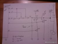
Zero-Draw, Solid State Contactor w/Precharge (Arduino)

I'm really curious how the linear reg works to boost with no inductor. A link to that cool part to check out would nice if you have the time to share it my friend.

I know how boot-strapping with a cap, diode, resistor, and something switching on an off works to climb voltage for driving a high-side FET, but it doesn't work if it can't tap that higher voltage side as well to enable it to climb it's supply high. This is how the high-side FETs are switched on an ebike controller as you know of course, and also the reason all current-control is handled on the low-side switching phase only with the top-side's comparatively weak power available for switching happening only at the commutation rate rather than the fast switching PWM required for current control that the low-side provides.

I know you can make a voltage doubler which switches in and out of being in series or parallel with charge storage caps rapidly to make higher voltage using no inductor, but it's typically very power hungry to use this method if you're working on sipping uA for your power budget, and the inductor type can be quite a bit higher efficiency topology as far as I understand it, but I'm no expert, more like an arm-chair putz talking about topology things I don't understand deeply enough to be talking about them, but hopefully you can occasionally pull a good idea out of the mess once in a while. :)
 
zombiess said:
What about using something like an A23 12V battery as a power source?

Interesting idea :)

612px-A23-open-closed.jpg


I did not realize those were 12V. At first I thought you were talking about a CR123 - which would also be a very nice fit. I have piles of the CR123's with the built in disk that offers LVC/HVC/Overcurrent protection

http://en.wikipedia.org/wiki/List_of_battery_sizes

At the moment I am just debating about whether I want to boost 3.3V to 9V, buck 9V to 3.3V, or run two separate supplies.

-methods
 
Personally, I don't see an issue with running off the V+ of the pack. The one extra wire doesn't need to be big and can be fed through a big resistor to make it safer. It does create some issues with references when trying to switch both charge and discharge paths, but the chinese have figured out this part.

A 12v regulator can cascade to a 5v or 3.3v for the processor. The 12v gate drive doesn't need very good regulation either.

With the main switch off, the drain could be zero.

One gate driver chip I've used in the past is the TPS2811. Typical drain 0.2uA. Not good for logic level input though, as it takes over half the supply voltage to trigger.
 
Thanks Fechter.
You are of course right... and the biasing is really not that complicated at all (one biases through the body diode of the other)... but I have it in my head that this will be a "wireless" device and be damned if I am not going to make it wireless :x . If I absolutely must draw power I will take it from across the open terminals with one of those awesome linear technology micro scavengers that can make 3.3V from like 20mV!

Looking more now at the larger lithium cells. A pouch on the bottom would be very modular and I could throw power conservation out the window. Build one of those sexy Linear Technology micro-power boost regulators.

Here is a random example http://www.linear.com/product/LTC3459
Lipo range in, 10V out, 80% efficient at 100uA (I am looking for one that runs over a lower range to get the eff up closer to 90%)

-methods
 
I've been researching several buck converter chips for a project lately. There are so many kick butt efficient chips available for cheap. Don't know why I haven't used them before. This thread has some nice think in it for sure.
 
That chip is amazingly cool, but it's just using a tiny inductor to make a very compact IC version of a conventional boost converter.

I want to see how the ones with no inductors work if they aren't just lossy stacks of capacitor voltage doublers or if someone has made some clever new method.
 
bearing said:
I haven't read the mass of text lately, so this may have been covered. I don't think it's hard to make a charge pump based gate driver. You need about 3 pins from the MCU and some small components. Or do you want the IC just to decrease part count?

Ok - going full circle-circle-circle and coming back around to this.
If I run the 328P at 3V it uses much less current than I though while "active" - so the idea of waking up more often to pump does not seem so bad.
I really like the idea of eliminating a buck or boost somewhere else (seems silly when the uController is there...)
I also like the idea of using a single 3V cell (and not some stack of cells)
If I do it right it might be SUPER efficient - since I really only have to turn it on or off a few times a day
You might be on to something here...

I am going to do it open loop tho :twisted:
Figure out the worst case leakage and multiply that by 3 or some nonsense. Avoid even turning on the ADC. Internal reference is only 1.2V so I would have to divide it down pretty far.

Lets have us a look... thanks for the idea.

-methods
 
Cool guys!
 
Arduino stroke material: 12 Volt Arduino-based Charge Pump

Damn that is easy :mrgreen:
@ 3V using 3 pins would get me 9V.... frigging perfect.
I can SLAM it off - so all good there.
I just need to add one more switch to allow me to turn it on more aggressiveness.

I dont know why I did not listen the first two times you said that I should do this :oops:
I am a hard headed bastard when I get to trying to solve a problem...

-methods
 
2013-03-08 22.07.09.jpg


Ok - I slapped together an arduino controlled charge pump that can get up to 9V, can turn on fast, and can turn off fast.

Ignore the fact that n-channel fets are used for the main fet turn off and the p-channel bias - I forgot my drive was only 3V and I was thinking I had 5V. I will replace those with NPN BJT's (shutter). Or maybe I can find a nice low signal set of fets that will work at 3V and come 2 to a package

Yea... so 3 pins to drive 3*3 up to 9V
One pin to short the gate of the main mosfet to turn it off
One pin to bias a P-Fet that turns the main mosfet on
Three caps and four diodes for the charge pump
A main storage cap for the 9V
Bias resistor and a Pfet for high side switching
Couple NPN's for controlling signals above 3V

yea - this could totally work
I will use a big-ass cap for the storage cap - charge that bad boy up and it will last a long time

Cycle would look something like this

* Cycle the pump and fill up the main cap
* hit the pchannel to turn on the main fet
* cycle the pump either on a cycle.... or bring back an ADC reading (barf)
* to turn off, turn off the pchannel (main fet stays on due to gate charge)
* immediately turn on the n-channel that shorts the gate (Note that we do not discharge the main 9V storage cap, only the gate charge)

I really dont want to add a pull-down resistor to the gate of the main fet... I know I should
Thinking that instead I might swap out the N-channel that shorts it with a depletion mode fet... or some shit like that.
Basically have the circuit rest with ground on the gate of the main fet - then an active signal needs to turn it on

Anyway - I have not thought this through. I just saw that Arduino circuit and started hacking things together. Generally I design like I code... successive approximation. I dont really care if it works on paper - when I build it the problems will quickly become apparent. And I dont simulate - simulation is masturbation.

-methods
 
I would consider optimizing the size of '9v storage cap' to be something where you only have to run the possibly inefficient charge pump more than once an hour for 1 second or something, then just coast on the cap bleeding down from the tiny gate leakage current and it's own cap's relatively tiny internal leakage current and the blocking diode's leakage current at this voltage. I have a hunch it's going to let the circuit use a lot less power wasted in that very clever and very cool charge pump while running to have something decently high capacity, possibly even being a useful application for one of the super tiny 4-series ultra-cap modules that do 10-11v-ish and have quite a lot of energy storage ability, like perhaps 1/10th of a tiny super tiny lithium coin-cell battery, which is overkill, but in the approximate ball-park for something that would let you only turn on the capacitor stacking charge pump very seldom, maybe only once a week or something if the ultra-cap's own internal leakage current was very low.

To do that cap optimization I believe you would want to look for the point that balances losses from the power supplies nearly-no-load current to run (which may be very small, in which case a smaller cap would make more sense in which case you should ignore my suggestion entirely, as when only drawing current here for the time its in operation, which should be at least a below 25% average duty cycle for gate needing high voltage vs not needing high-voltage, it starts to matter even less. Yep, found and skimmed this paper on charge-pump method of operation details, it's a lot trickier than you may think it looks in operation and has decent resistive component loss, though more efficient than I had thought it would be and better than the other cap-only voltage doubler circuits I've seen with less current/voltage ripple as well using 3 cap phases (which also helps it get the voltage it needs).

http://powerelectronics.com/passive-components/calculating-essential-charge-pump-parameters

Seems like perhaps just a small-ish low-leakage current cap would be better there than an ultracap after thinking it through aloud.
 
Thanks guys. Henry has been here all day and it is the first day I have not worked on the circuit. Today was awesome tho - Henry fired up Lukes CNC router and showed me how to make something up on Solidworks, pimp it out in Gibbs, then machine it in the real world. It came out awesome and I can totally see how to do it. Up till now a bunch of old timers were trying to tell me I should do shit by hand in G-code :roll: phfffttt.... whatever :x

We then went to the beach at -0.5' low tide and I finger'ed an annenomi. :)

Then at like midnight we worked through all the stages of that charge pump (which is pure awesomeness) to prove to ourselves that it would work - and while doing that it hit me like a ton of bricks that I dont need those three control fets on the output of my circuit....

I could totally replace all three of those fets (the two N-Channel and the P-channel) with a single ultra-low power 1uA OpAmp. Yea... Yea... I know they dont like to drive capacities loads... but it will totally work. I will power it from the 9V. If I send it a logic low it will pull the main output fet down. If I send it a logic high it will rail 9V into the fet.

Simple

Two parts - OpAmp and a bypass cap
Only one uController pin instead of two
No timing issues
No leakage through the P-Fet pull up resistor

Ok - might take 3 parts as I may need to do something tricky to get the OpAmp to slam as much current as I want it to (could be a cap or a BJT - not sure how I am going to do it yet - have to research the latest in OpAmp technology)

I will click the links that Luke and Fechter supplied tomorrow morning... Thanks guys.

-methods
 
OpAmp is looking TOTALLY do'able

0.6uA standby current
Frequency response up to 100MHZ (May need to switch to a high speed high voltage comparator)
I will just set it up to rail on a cmos input

I need to go figure out the worst case fet array that I am going to have and how fast I really want to turn those on. I am *not* going to PWM these - and super fast turn-on can be a real bummer - so... yea... It will probably be easier to just test than to dig through the bullshit datasheets and try to figure out what is real and what is sales talk. If it does not burn things up at 100A, or make insane ringing at 150V, or fail to bleed the gate on a power failure...

Might go look at some high-speed, high voltage comparators too.

What is really important to me (whatever device I use) is how it behaves when power is lost. Whatever it is it needs to drain the gate charge pretty fast. I dont think that will be a problem at all - and I really dont want to hang a gate discharge resistor out there as it is just wasteful for an application like this.

Hmmm maybe I can set up the uController Brown Out Detector to slam the fet closed in the case of an emergency.

-methods
 
I think you can use an NPN/PNP emitter follower (totem pole) to add to the "umph" of your micro power op amp.
 
I am racking my brain... I can feel it on the tip of my tongue... There are so many devices that can meet this requirement

* Cmos input from a uController
* Switch 9V
* Sink and source relatively hard
* super low quiescent current
* must discharge the gate charge when power is lost

- OpAmp
- high voltage comparitor
- high voltage hex buffer
- insane low power gate driver (50uA is the lowest I have found so far - I want less than 10uA

Open collector output is not that useful (otherwise I could just use an LV fet or BJT

So frigging close - solve this last part of the riddle and I can start prototyping.

-methods
 
bigmoose said:
I think you can use an NPN/PNP emitter follower (totem pole) to add to the "umph" of your micro power op amp.

thanks,
-methods
 
There is a -0.2' low tide at 16:30 today. At this particular location you can walk out a hundred yards into tide pools. Going to strap the dirt magnet to my chest and go out there.

Same location, time before last, higher tide

2013-02-022.jpg
2013-02-024.jpg
2013-02-032.jpg
2013-02-037.jpg

Henry and I were there yesterday - found this fossil. Cliff sides are like the rings in a tree - covered in a story

2013-03-09 14.55.02.jpg
2013-03-09 14.55.20.jpg

-methods
 
methods said:
There is a -0.2' low tide at 16:30 today. At this particular location you can walk out a hundred yards into tide pools. Going to strap the dirt magnet to my chest and go out there.

Same location, time before last, higher tide

View attachment 5


-methods
EDIT: not sure how to make pics work in my quotes but you say "this is the future"?

You're totaly the kind of guy to say something like that when it could be just BS and you like to make simple folk like me wonder WTF is that?
 
Rusting ford V8 FE series big block Im guessing.
 
Yeh it looks like a V8 now that you point it out. The way the valves are It kinda looks like a hemi but the stamp pad is missing from the front of the block. I dont know my fords well so SCJ or something with intake and ex valves on a different center line.... Cool Yup definatly the future
Actulay it looks like it could be a 426 lol just backwards. http://www.google.ca/imgres?imgurl=http://www.igstest.com/71cuda/projectSAVE/426hemi10.jpg&imgrefurl=http://www.igstest.com/71cuda/projectSAVE/&h=525&w=700&sz=112&tbnid=fqNeS1qpK0ZQBM:&tbnh=91&tbnw=121&zoom=1&usg=__wijF5CJf0yW6aaBXudxRZPhV4vE=&docid=KaGgH-M_DmVl5M&hl=en&sa=X&ei=lU09UZPwM4muqQGProDYAg&ved=0CFAQ9QEwCg&dur=311
 
Back
Top