DIY 6FET Controller help

HighHopes said:
I was thinking more on the sinusoidal case, and now I find possible that HighHopes's formula is the correct one for the fully symmetrical sinusoidal drive, and mine is not applicable in this case

lol no worries. we're just discussing theory.

That's correct! :)
But I didn't say I agree with your calculation, just that it needs more investigation for me to understand the 3P sinusoidal case. I started thinking on this because Zombiess told me I would need only 20..30uF based on your formula, that I strongly doubted, and I don't want the people here to be misguided with a wrong calculation... In my case I need at least a 10 times bigger capacitor if it is a film cap.
Of course I'm sure your circuit works, but I'm pretty sure that in the worst case situations your ripple current is a lot larger than your estimation. Unfortunately measuring the ripple current waveform is not easy when the capacitors are soldered on the board.
As you see I also simplified a lot in my model, but in my opinion you ignored the most important part of the capacitor current, that is the DC component of the phase current, that I did not ignore. Your calculation is based on only the phase ripple current, because you said your worst case simulation started at bemf=0, i=0 and maximum torque applied. But as I see, it will not give the worst case capacitor ripple current, because when the phase current is at maximum, 100..200A or more, it cannot be ignored, this is much more than the phase ripple current.
And now I see it is the case for the sinusoidal drive, too: just imagine when you switch any of the phases from low to high or high to low voltage, then the phase current of that phase is added to or subtracted from the bridge supply current via the high side FET of that phase. This change in the current is the ripple in the DC bus current, and its level is the actual phase current along the sine wave. If the peak phase is 200A, then it is between -200 and +200A. During one PWM period there is a low to high and a high to low change on every phase, that gives a current curve from 0A to the maximum, and this curve dynamically changes along the sine wave. The AC component of this curve is the capacitor peak-to-peak ripple current, and its RMS is what we are interested in. Finding the maximum ripple would be an optimization task (function of the voltage sine wave amplitude, the phase degree and maybe other variables), but my calculation for 1 phase DC gives an upper approximation of the worst case, this is how I see it.
 
Alan B said:
Seems to me that some of the controllers we use have built-in ripple detection fault tripping. So they must be monitoring that. Would not be hard to build a circuit to do, might be useful in a development controller.

Is that for voltage or current?
For voltage it is easy. And I have that 1mOhm resistor on the GND bus between the cap and the bridge, that I like, so I will be able to measure the ripple current, too :)
 
HighHopes said:
looks ilke you are using DC link negative terminal as connected also to your digital ground. if you do that, there is no need for half the ACP-333J you have on the board and also you will be limited in the power range (dunno if you will get the 150A you want).

once you fix that problem, the ground loop issue will go away.

also, are your mosfets going to share a common heatsink? they should.

also, you might consider making the void around DC link cap terminals a bit bigger. bad for canceling magnetic fields, but in this case the reduce chance of flash over due to cap leg soldering blob would probably be worth it.

Thanks HH , I will seperate Batt- from Digital-GND using a DC/DC convertor so Digital Gnd will be floating.
I see from the gate-driver-ground-planes-draft.jpg (that you asked zombiess to post), the small DC/DC supplies for the GateDrivers ground plane are
connected to main BATT GND, and on my layout I have them connected to Digital-GND which will now be floating. Do you see a issue with this?

I will have a common heatsink for the MOSFETs and plan to fit a temperature sensor as well.
 
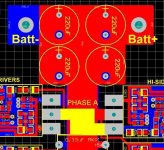
I think your power caps could have a better orientation, SjwNz. You're forcing the current to make "90º turns" and the path through the several caps is not symmetric, some paths are longer in a very assymetric way, which means the transient ripple work is not evenly distributed to the several caps. Ideally the power input would come from the top and the caps leads would be aligned vertically to reduce loop area. This is just subjective interpretation from my part, may not be that relevant.

peters said:
Alan B said:
Seems to me that some of the controllers we use have built-in ripple detection fault tripping. So they must be monitoring that. Would not be hard to build a circuit to do, might be useful in a development controller.

Is that for voltage or current?
For voltage it is easy. And I have that 1mOhm resistor on the GND bus between the cap and the bridge, that I like, so I will be able to measure the ripple current, too :)
That measures phase ripple/current, but for cap ripple you still need to measure bat current at "the same" time.
 
peters said:
I started thinking on this because Zombiess told me I would need only 20..30uF based on your formula, that I strongly doubted, and I don't want the people here to be misguided with a wrong calculation... In my case I need at least a 10 times bigger capacitor if it is a film cap.

I wasn't telling you that you only needed that much, just going off the information I had on hand. As a designer it's up to you to determine what your application requires.

I said the following
I suspect you might be OK with a 20-30uF cap of the proper type, but the math must be done. Electrolytic a are something you should probably stay away from for DC Link usage.

I saw a 6 TO-247 MOSFET layout which typically means you'll probably be running a max of about 50A per FET continuous which led me to believe you were designing a 2-3kw inverter. I was just SWAG'ing what I thought the minimum capacitance might need to be with good high current PP caps. I'm not a pro at this, but have done some hands on bench testing. I really need to do more simulations since I'm really lacking that skill, I just started learning it a little bit recently.

It did start a new discussion and I've learned some more info I didn't previously know so I'm happy. Designing inverters is a real challenge, so much to learn.
 
No problem, Zombiess. HighHope's formula really gives 20-30uF, that was my issue. Others using the formula may have problems if they apply it for their design, in my opinion.
It is a good learning and practicing time for me, too.
But I finish this here, it is SjwNz's topic. :)

Btw I'm targeting 100A, anything above that is nice to have. And I will try ACPL-H342 gate drivers with isolation and miller clamp, that is what I was missing on my previous board.
 
SjwNz, don't you think you want to change to higher supply voltage later? Because the DC/DC converter input voltage is the only limitation on your board, as I see. There are higher voltage ones, too.

If you don't find an isolated DC/DC for your voltage, then a filter made of two L-s (or ferrite beads) and a C can be also appropriate, tuned to filter the MOSFET switching transients, that is around 1MHz and higher, because it makes the problems, at least according to my experience. One L (or ferrite) would be on the power supply line and the other one on the GND, and after them the C. Then the DC voltage is not isolated, but it isolates the critical frequencies. It is just my idea, not a proven circuit, but it should work and I will try this on my board.
 
peters said:
SjwNz, don't you think you want to change to higher supply voltage later? Because the DC/DC converter input voltage is the only limitation on your board, as I see. There are higher voltage ones, too.

I found a DC/DC supply with a 18v to 72Volt input range and I only plan on running up to 50Volts and have no plans to go any higher in voltage.

peters said:
If you don't find an isolated DC/DC for your voltage, then a filter made of two L-s (or ferrite beads) and a C can be also appropriate, tuned to filter the MOSFET switching transients, that is around 1MHz and higher, because it makes the problems, at least according to my experience. One L (or ferrite) would be on the power supply line and the other one on the GND, and after them the C. Then the DC voltage is not isolated, but it isolates the critical frequencies. It is just my idea, not a proven circuit, but it should work and I will try this on my board.

Maybe a common mode coke will be better for this instead of separate 2 coils ? Think I will stick with the DC/DC supply for now to isolate the digital gnd from battery gnd as I dont want to stray off the path to much that may make my controller blow up. Assuming I am on the correct path :D
 
SjwNz said:
Maybe a common mode coke will be better for this instead of separate 2 coils ? Think I will stick with the DC/DC supply for now to isolate the digital gnd from battery gnd as I dont want to stay off the path to much that may make my controller blow up. Assuming I am on the correct path :D
Yes, for sure.
And I will examine the common mode choke for my board, thx for the tip.
 
Njay said:
I think your power caps could have a better orientation, SjwNz. You're forcing the current to make "90º turns" and the path through the several caps is not symmetric, some paths are longer in a very assymetric way, which means the transient ripple work is not evenly distributed to the several caps. Ideally the power input would come from the top and the caps leads would be aligned vertically to reduce loop area. This is just subjective interpretation from my part, may not be that relevant.

I think I remember zombiess talking about cap orientation somewhere as well on another thread. So I would have to rotate the caps 90degs to be inline
and place the power Inputs at the top, something like this ?

ScreenShot008b.jpg
 
Njay said:
See doc 4) here: http://endless-sphere.com/forums/viewtopic.php?f=30&t=61199
Useful documents, thanks. (the first one is missing).

Concerning the low voltage DC/DC converters for the gate drivers, usually they have 30-60pF isolation capacitance, so there is a high frequency coupling between the 2 sides. I don't know how much problem it is or the best solution to avoid or limit it, but compared to this, the capacitance between the 2 opposite sides of a 1.6mm FR4 PCB is only 3pF/cm2 (10x10mm). Any idea?
 
DC/DC power supply capacitance (primary to secondary) is a BIG deal for high voltage application (say >300V). or low(er) voltage with fast switching mosfets.. whatever gives you high dV/dt.

for product development, i design my own transformers and i have a goal of 5pF max. it is acheivable with a torroid core or very careful E-core winding.

for your typical DIY project, probably you can get away with 30pF. its hard to say. if there is a problem you just slow down the switching, check the temperature rise of mosfet and if not OK, lower the phase current. done.
 
I see, thanks!
Anyway, due to the lack of space on my board I'll probably use bootstrap with low capacity diodes for the high side.
 
What do you think of the hall sensor power supply and signals?
The wires are close to the motor phase wires in the cable, so there is some coupling. I don't know how much it is, but the cable is long and there is high dV/dt. It may generate noise on the microcontroller GND and power supply, so maybe it would be useful to isolate the the hall sensor power supply and adding optocouplers on the hall inputs on the controller board.
Do you think it is necessary or not?
 
i don't have the schematic or layout files of this design so not sure the specific case.

in general, you should supply any sensor that is remove with its own power supply. how to do that exactly, actually would be another discussion about power supply archetecture. even in my own EV design i don't think i have it quite right yet. i'm torn between doing it proper and doing it easy. because in my experience a hall effect sensor is fairly tolerant to a noisy environment. between the sensor and your analog signal conditioning circuit, not so much.. but between the high power bridge and the current sensor, pretty tolerant.

for control power, you need at least one level of isolation between the battery bank and your digital/analog power supply. but after that one level of isolation, it is enough. let's say you take 72V battery pack to +12V control power (this would be regulated & isolated). from this power supply you would then make a 12V to +5V non-isolated supply for your external sensor's use (including the current sensor you asked about) and then an LDO +5V to 3.3V for your digital power. so you can see that the +5V or +3.3V are neither isolated supplies themselves per say, but both are isolated with respect to the 72V battery pack. the point is that it IS important that sensors external to your main PCB are supplied by a separate power rail.

if you're still reading this then you're probably wondering where the gate driver power supply(s) come in. in this scenario, they would be +12V to whatever votlage you want for your gate driver but the supply is design to be isolated, unregulated. of course you need 6 of these (or 3 if you have low power & mediocre performance on your mind). the gate driver power supplies are purposely made to be unregulated due to the power supply's design requirement of < 5pF primary-to-secondary total capacitance. you basically can not afford the amount of parasitic cap that comes along with trying to make a feedback circuit across the isolated boundary. you could also say now that there are TWO layers of isolation between the gate driver power rail and the battery pack; which is actually fairly common design requirement.

are you still following me?

futurama and i talked at length about this so he might have some handy diagrams to share.
 
I read of course. But I mean the position hall sensors inside the hub motor, not the current sensors. For these I find the isolation is also better, not only for EMI, but if the phase wires are shorted to these hall signals due to a failure, then isolation prevents burning the other low voltage circuits. My long term plan is sensorless FOC, but until it is implemented I will need these position sensors.

Concerning the gate driver supply I'm thinking on another option: 3 independent linear power supplies directly at the low side FETs sources on the power board. It is probably not usual, but it would not need more than 10-15mA per MOSFET, taking into account the gate driver supply current and the gate charge at 20kHz PWM. It is altogether 6..9W for 6 FETs from 100V, that is not much loss compared to the few kW-s output power, and it simplifies the power distribution and there is no capacitive coupling to the analog and digital circuits via these power supplies at all. The circuit would be a simple zener diode regulator with an emitter follower transistor and a few resistors and an output capacitor, and the transistors can be insulated TO-220 packages mounted on the common heatsink.
 
i don't know for hall sensors, i never used them. i used either a precision high speed resolver, or sensorless.
 
i always use DC too. old habbits die hard i guess
 
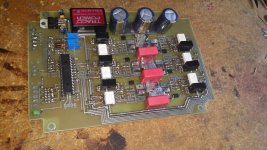
Looking good, SjwNz :D

As HighHopes mentioned, I do have some artwork of a supply system, but it seems like you have done it right. I guess the TRACO POWER is a regulated module, right?

What DC link capacitors are you using (manufacturer and part number)?
 
Back
Top