20Kw motor and 300A ESC (ultralight aircraft propulsion system)

mxlemming said:
liveforphysics said:
Great job in your power bus packaging. You've got way above average electrical and thermal conductivity, and tight inductance. I'm excited to see how they perform, I may need to make or buy some for my own projects.

Been wondering, what commutation control would you pair this with/what do you generally use? Lebowski? VESC? ST/TI/infineon? Custom?

FOC, BLDC or other?

I leave it to Arlin and and Jeremy on this forum, and stay focused on making the worlds safest and most environmentally rugged batteries on the planet for clients.
 
mxlemming said:
You might have overloaded it but I have had plenty of these die and I definitely have not been overloading them at 16 and 20s. I have a 2r2 resistor, 85Vtvs diode and 2.2uF ceramics in front of my ones inputs... They still die.

I think the bottom line is that where other manufacturers are optimistic with ratings, TI simply lie through their teeth. They recommend it for 48V systems.

The 516x series isn't much better in my experience, and TI MOSFETs are rated 200A for the same package limit as others rate 120, and i know from first hand experience the legs rapidly fuse at this current. They have an appnote for those 100V FETs that says "excellent choice for traction vehicles, 200A rating, we used 36 of them to make a 48V120A inverter".

You might want to swallow hard and pay the premium for the 140V linear tech parts, or buy a dcdc module.

Il be designing them out of all my future devices. In fact I'll be avoiding absolutely all TI parts, I frankly trust them less than the Chinesium no brands.

Incidentally, there are fake 5017s out there but mine were direct from TI's web store.

I will to switch to a DC-DC module, 15W (15V/1A), i will need in the future some extra power, space i have enough to fit it inside the case.
I had enough trouble with LM5017, i kinda liked it, to bad that is not reliable... I measured 0.18A at output of the buck, just GLCD draws 0.1A measured at full brightness. The LM5017 has overcurent protection 0.8A, there is no way to pull 1.4A thru it without blasting itself into oblivion. So the chip was not overloaded, it has carp chip reliability.
Up to this point i only worked with small 1W DC-DC 12V-12V from aimtec.
If you have any sugestions of such DC-DC converter modules, Vin 30 to 150V capable of 15W. I did a bit of search but is hard to find some in stock these days... :roll:
 
https://www.digikey.co.uk/en/products/detail/cui-inc/PQDE6W-Q110-S12-D/13178541

Try something like this?

There are actually a lot of dcdc modules of you're willing to pay upwards of 15usd, and loads of sketchy looking ones on AliExpress is you want to pay 1usd.

Other option I've been considering is running a tiny usb charger to create 5V then boosting to 12V. Those things are rated for 84 to 265V usually. Most will happily accept DC input, but not all will work at the lower end of your battery voltage.

Other nice thing about these options is that they're isolated so when they fail, they probably fail safe and just stop creating voltage rather than dumping the battery into your gate drivers.

This is one of those things actually that zombies told me over a year ago that he gladly pays $$$ for isolated bricks from (ltc? Can't remember...) And i was like nah, i got me lm5017s that work fine.

And they did, while I was running them at 55V with over voltage protection set at 65... But when I went up to 16 and 20s, and started using VESC code, they started to become disposable.
 
I'm back with some interesting findings and also problems to solve. The mod to Dc to Dc converter module was a success, the 40-160v in to 12v out 6w, the one suggested by mxlemming.
Now the findings: the redesigned power section seems to be switching nice and clean, it is not quite there yet, i did a loaded motor test, and at 40A after 3 sec, it failed. I found a shorted phase module, and that made me investigate and do a lot of measuring. I scoped the high side Vgs when low side fet is switching, i suspected parasitic turn on due to miller (reverse treansfer capacitance), and sure enough i found that high side Vgs is rising above Vth and it turns on for a brief 50ns, cross conduction, this finding is backed up by a current measurement, witch showed some crazy current spikes at turn on, plus the fets do heat up fast if i try to run at 35A just below where it failed (40A). That turn on ringing that i found a few months ago, i believe it is caused by this cross condition event. Here are a few scope shots, all shots low side switching 440A 92V duble pulse test.
First: yellow low side Vds but mirrored (probe gnd on sw node), green high side Vgs
IMG_20220323_125657.jpg
Zoomed turn on
IMG_20220323_125705.jpg
Zoomed turn off
IMG_20220323_125712.jpg
Second: yellow high side Vds as low side shitches, green curent(a wire as shunt)
IMG_20220323_125637.jpg
Third: yellow low side Vds, green Vbus(92v) on fet lege, ripple
IMG_20220323_125628.jpg
Now the hard bit, how do i fix it?, i have a few options, best optionis to upgatade gate drive to have miller clamp, other options slow down switching, or ad Cgs caps.
I tryed Cgs (10nF in resies with 4,7r) on low side, and it does improve and slows down switching at turn on, but introduces some unwanted ringing at turn off, here is a shots, yellow low side Vds green low side Vgs.
IMG_20220323_125831.jpg
IMG_20220323_125750.jpg
Here is the miller effect on high side Vgs it has lower amplitude
IMG_20220323_125856.jpg
As much as i hate to admit the ir2110 alone might not be enough to drive this fets, they need more complex driver, with miller clamp 2 stage turn on and off. So before i start redesign, i will do a test with the clamped (thru 1.1r ) high side Vgs of the phase that is tested, to prove that a milker clamp is needed, then i will star thinking on what to do.
So please take a look, and comnent what you guys think on this. Thanks in advance.
 
i measured high side Vgs while being clamped thru 2.2r, low side switching, there is a big improvement Vgs spike is only 2,2V is far from Vth, even the Vbus on fets legs ripple is smaller.
So the conclusion is: gate driver redesign, i will go with TD350E with 5A buster stage, active miller clamp and desat.
The previous version V1,2 with slower fets (4468), the IR2110 driver was just enough, because fets ware slow and they accepted 33nF Cgs to stop ringhing and miller reverse transfer....but these faster fets 150p220 do not work that way...
You guys did point out in the beginning that more complex gate drive is needed, back then i was so fixated that it might just work, because it did on V1.2, but here it is not the case.
So I'l go the extra mile and do a good job and stop messing around with not enough gate drive circuitry.
All tests low side switching DPT 440A 92V.
Yellow low side Vds mirrored, green high side Vgs
dso_01_01_00_32_01.jpg
Zoomed
dso_01_01_00_23_44.jpg
Yellow Low side switching, green Vbus ripple
 

Attachments

  • dso_01_01_00_11_02.jpg
    dso_01_01_00_11_02.jpg
    111.4 KB · Views: 1,366
Hi mihai,

Shame it's not working so well. There was so much promise from the pulse tests.

Regarding the miller effect, I don't think this is what you're seeing. If you look to IMG_20220323_125750, you can see there's an offset between the gate traces before and after the switch of maybe 1V (extrapolate the lines through the noisy but) That's the miller capacitance. The transient stuff that's over in 100ns is inductive.

It's not yet clear to me whether inductive effects turn the FETs or if they're invisible to the silicon. My hunch is that they do not turn it on.

IMG_20220323_125637 is quite horrible and unexplained. Why is the current oscillating so wildly during a "steady" region? Where is the measurement taken?

My gut instinct is that your problem does not lie in the individual stages, but rather the combination of all 3 being strapped together and being driven by such cheap gate drivers that have low drive capability and unknown behaviour during moderately large ground offsets.

It probably would be solved by the isolated gate drivers, like td350e but not because of the miller clamp.
 
mxlemming said:
IMG_20220323_125637 is quite horrible and unexplained. Why is the current oscillating so wildly during a "steady" region? Where is the measurement taken?

That was a failed attempt to measure current on the phase with 10cm long 5sqmm wire as a shunt. And the noise from motor coils made it unusable...

mxlemming said:
My gut instinct is that your problem does not lie in the individual stages, but rather the combination of all 3 being strapped together and being driven by such cheap gate drivers that have low drive capability and unknown behaviour during moderately large ground offsets.

It probably would be solved by the isolated gate drivers, like td350e but not because of the miller clamp.

If you look at the shot IMG_20220323_125705, where high side was only held down by the drivers thru 12r each of the 3 gates, the spike goes over 10v, and the 150p220 has gate threshold from min 3v to max 4.6v, and from the datasheet for id 100A Vgs needs to be about 5.5v, so for a few tens of ns they do turn on and that is reflected on the Vbus ripple. In the test with each of 3 high side gates clamped down with a 2,2r, the Vgs spike is only 2,2v and the Vbus ripple is also 2v lower in amplitude. This cross conduction event in this 440A DPT is not that obvious and it does not affect that much, but when running the motor with PWM of 16khz, and at 40A it sure does affect a lot, fets do heat up really fast, and in 3 sec they pop.
 
I'm back with progress, i made the gate driver board layout, it is mainly based on the schematic presented here on the first post (zombiess) https://endless-sphere.com/forums/viewtopic.php?f=30&t=58341 . The output tranzistors are chosen to be SMD 2SD2118 and 2SB1412, and the isolated DC-DC converters are ISE1215A, the rest is pretty much what is in that schematic, except the gate resistor values. When i redesigned the power section, i made it such a way, that a gate driver board to be fixed on top of each half bridge board. I made the switching loop as tight as possible considering the board is 65x50mm, so here it is the layout.
If you have any thing to add or comment please fell free to do so.
gate driver board1.jpg
 
I'd encourage you to practice more isolation techniques. They can really reduce noise by minimizing coupling. I've found that booster stages haven't been needed when switching at normal speeds, even with multiple parallel devices. They may be needed for some devices, so it's a good idea to do the math on gate charge.

Practice risk management, it dramatically increases chances of success.
 
zombiess said:
I'd encourage you to practice more isolation techniques. They can really reduce noise by minimizing coupling. I've found that booster stages haven't been needed when switching at normal speeds, even with multiple parallel devices. They may be needed for some devices, so it's a good idea to do the math on gate charge.

Practice risk management, it dramatically increases chances of success.

Thank you for your reply. I chosen to use bust stage, becouse of peek current when chaging the gates being over 4 amps, and most inportant the hold low gates voltages of outlow and clamp (about 1,...v) of the TD350E. The fets being very fast and snappy, i wanted some good and strong gate drive, with hold low in the order of 0.3 to 0.5 v (Vsat of the bust stage) , the IR2110 was not enough to hold gate low, and i suspected that clamp of the td350e might not be too, so then boost stage to be sure.
I have a question about desat, how do you calculate or choose the zenner in the desat circuit for the max current, i kind of understand the purpuse of that zenner, but if you coud please explain a bit how to choose the right zenner for a given current. Thank you.
 
Mihai_F said:
Thank you for your reply. I chosen to use bust stage, becouse of peek current when chaging the gates being over 4 amps, and most inportant the hold low gates voltages of outlow and clamp (about 1,...v) of the TD350E. The fets being very fast and snappy, i wanted some good and strong gate drive, with hold low in the order of 0.3 to 0.5 v (Vsat of the bust stage) , the IR2110 was not enough to hold gate low, and i suspected that clamp of the td350e might not be too, so then boost stage to be sure.
I have a question about desat, how do you calculate or choose the zenner in the desat circuit for the max current, i kind of understand the purpuse of that zenner, but if you coud please explain a bit how to choose the right zenner for a given current. Thank you.

The IR2110 is no where near suitable for your application.

The zener is chosen based on the RDSon of the devices you are switching. The desat pin outputs 7.2V @ 250uA, so your choice of zener can get interesting as most don't supply ratings for < 1mA. What I've done is buy an assortment of voltage ranges and test them through double pulse testing by sneaking up on my target trigger current. Keep in mind that during high dI/dt events such as shoot through, the current will spike much higher than what you set it at during testing. Generally I'll target 150-200% of my max safe operating current to prevent false triggering. You also need to remember that the RDSon is going to vary with temperature, so if your MOSFET is running hot, the desat trigger level will be lower and the opposite holds true when cold. The lower the RDSon value is of the MOSFET, the more difficult it is to precisely tune the trigger event. Once you figure out your values for a single device, you can parallel as many as you want and the trigger level stays the same per device. So if you set it to trigger at 300A on a single device and you parallel 3 devices, your new trigger level is 900A, but generally it's better practice to derate, especially for aviation use.

Don't design a component, design a system. Control every signal line, always know it's state and what the result of that state is.
 
=m :mrgreen: xlemming post_id=1687106 time=1637075629 user_id=73685]
This is generally how I would aim to do it if i played with through hole FETs.

However, your copying zombiess multi board approach probably necessitates copying his use of isolation as well.

There are simpler isolated gate drivers than the ones peters and zombies use, ucc21520 for example, but availability might be tricky now and you lose the desaturation protection.

I'm fully agreeing with zombies assessment.

My only concern with td350e is that their pull down capability doesn't seem to be much greater than the ir2110s, which is why you're having to add extra transistors etc...

But there are parts from infineon and on semi that have stronger pull out of the box. I think you could simplify this a bit. Simplification, as well as isolation and risk management increases chance of success.

I'd meant a few weeks back to make some more notes on the waveforms your found. You've all but fixed it I suspect with the isolated drivers but I think it's important to note a few things:
IMG_20220414_055319_121.jpg
In my screenshot of your scope you can see the Miller effect between the two red lines I've drawn. It's about 1.5V. this is about what I'd expect for that MOSFET and bus voltage.

The high frequency stuff is the result of the Miller capacitance turning the FET on and off as the voltage falls. I don't know if it's especially harmful or not. It's certainly going to result in more energy dissipated in the junction than a smooth transition since you're charging and discharging the output capacitance multiple times and that energy is dumped into the junction but whether it's too much...

The next thing I note is your gate rise time constant. About 400ns from eye. That's quite slow already. If you slow it down even more you're going to have issues with dead time, which I presume you must already be running about 1.5us or so. That's a lot of dead time, it directly affects your output voltage. Dead time is effectively an opposite voltage so rather than driving there motor during the dead time it's... Anti driving it. If you're running 15khzpwm for example, 1.5us represents 5% voltage loss.

Despite your slow time constant on the gate, your FET is still switching in about 50ns. Clearly slowing down the gate more is not going to help things much but will have serious detrimental effects. I would speculate that the high frequency noise during the switch will be amplified and last longer... More damaging to the FET

The higher amplitude noises you've labeled as Miller in various screenshots of the scope above are 100% not Miller effect, they're inductive effects. If you try to treat them as Miller related problems, you will only succeed by sheer luck if atall, and in the process cement incorrect understanding.
 
mxlemming said:
I'm fully agreeing with zombies assessment.

My only concern with td350e is that their pull down capability doesn't seem to be much greater than the ir2110s, which is why you're having to add extra transistors etc...

The next thing I note is your gate rise time constant. About 400ns from eye. That's quite slow already. If you slow it down even more you're going to have issues with dead time, which I presume you must already be running about 1.5us or so. That's a lot of dead time, it directly affects your output voltage. Dead time is effectively an opposite voltage so rather than driving there motor during the dead time it's... Anti driving it. If you're running 15khzpwm for example, 1.5us represents 5% voltage loss.

Despite your slow time constant on the gate, your FET is still switching in about 50ns. Clearly slowing down the gate more is not going to help things much but will have serious detrimental effects. I would speculate that the high frequency noise during the switch will be amplified and last longer... More damaging to the FET

The higher amplitude noises you've labeled as Miller in various screenshots of the scope above are 100% not Miller effect, they're inductive effects. If you try to treat them as Miller related problems, you will only succeed by sheer luck if atall, and in the process cement incorrect understanding.

yeah, now it is clear that ir2110s barely had enough grunt to switch the gates fast enough, hence 400ns initial ramp up, it is clearly not enough gate drive function.
So, what you say, it is 100% NOT miller effect, it is inductive effects (the gate spikes), so they mess around with the gate voltage and produce the shoot thru event? sounds resonable, that inductance might come from the long twisted wires (few 4 or 5 cm) from gate drivers to the power board, with the new gate driver board witch will be mounted on top of power board that distance will be eliminated almost completely, and 5A gate drive punch will certenaly be able to switch the gates faster than 400ns, plus the clamp function keeping the gates voltages secured down.
 
zombiess said:
The zener is chosen based on the RDSon of the devices you are switching. The desat pin outputs 7.2V @ 250uA, so your choice of zener can get interesting as most don't supply ratings for < 1mA. What I've done is buy an assortment of voltage ranges and test them through double pulse testing by sneaking up on my target trigger current. Keep in mind that during high dI/dt events such as shoot through, the current will spike much higher than what you set it at during testing. Generally I'll target 150-200% of my max safe operating current to prevent false triggering. You also need to remember that the RDSon is going to vary with temperature, so if your MOSFET is running hot, the desat trigger level will be lower and the opposite holds true when cold. The lower the RDSon value is of the MOSFET, the more difficult it is to precisely tune the trigger event. Once you figure out your values for a single device, you can parallel as many as you want and the trigger level stays the same per device. So if you set it to trigger at 300A on a single device and you parallel 3 devices, your new trigger level is 900A, but generally it's better practice to derate, especially for aviation use.

Don't design a component, design a system. Control every signal line, always know it's state and what the result of that state is.

Thanks for your explanation, i'l try that, i'll test it.
Yeah, with designing a system, i'm on a learning curve, i had a some failures or not successful attempts, hopefully i'l learn what NOT to do in the future. I did a lot of learning and still do, my knowledge doubled since i'm around this forum, did a ton of reading here. Electronics design is a vast knowledge domain, clearly much more vast that i anticipated at the start at my project years ago :D.
 
yeah, now it is clear that ir2110s barely had enough grunt to switch the gates fast enough, hence 400ns initial ramp up, it is clearly not enough gate drive function.
So, what you say, it is 100% NOT miller effect, it is inductive effects (the gate spikes), so they mess around with the gate voltage and produce the shoot thru event? sounds resonable, that inductance might come from the long twisted wires (few 4 or 5 cm) from gate drivers to the power board, with the new gate driver board witch will be mounted on top of power board that distance will be eliminated almost completely, and 5A gate drive punch will certenaly be able to switch the gates faster than 400ns, plus the clamp function keeping the gates voltages secured down.
I don't think it's the gate driver lines, it's most likely the inductance between the boards. When you switch 400A it changes from flowing through the high side of the bus to flowing through the low side in nano seconds. The inductance of that link absolutely will cause a significant bounce.

The gate drivers can only tolerate a few volts difference between signal ground and logic ground... 6 from memory. Beyond that, the signal propagation doesn't work and there's parasitic for behavior and... Generally undefined.

The isolation removes this constraint. It may not remove it from your scope shots but it will improve functionality.
 
I'm back with progress, i completely redesign the command and driver boads, i assembled everything, all checks out fine, there ware a few things here in there to fix. Did not have time to scope any waveforms, just measured functionality with dmm, i finished late last night. Here are a few pictures, it looks sleek 😉. I'l get back soon with measurements and lots of details.
IMG_20220506_180122.jpg
IMG_20220506_180159.jpg
IMG_20220506_133529.jpg
IMG_20220506_133517.jpg
IMG_20220506_130757.jpg
IMG_20220505_104424.jpg
 
Beautiful work my friend! Let us know how it dynos!
 
hy guys,
i'm back with measurements, i have some good news and some confusing ones, so here it is:
the controller spins the motor,
i made the double pulse test as before, the setup is as follows, low side pulsed, 90v bus, 10uH 6mohm inductor (the motor), snubbers with 0.75 dumping on Ls and Hs, gates tied together thru 1 ohm resistor then Rgate 2.2R for Ton and Toff, with active miller clamp, without 2 level turn off, desat is used (5v1 zenner) but not configured right at this time (needs lower zenner voltage), yellow trace is Vds greed trace is Vgs.
i started testing with some short 600ns pulses, all was ok-ish, (only this shot has Vgs yellow trace), i say ok-ish because Vgs rises nicely then once is up it has a sharp short drop to 0 then back up, that drop does not seem to be in the miller plateau but as you will see in further shots it is located in the region the Vds drops down fast, so i think when Vds drops fast it pulls down the gate voltage or something, with the previous gate drivers in that same position was some crazy ringing.
the 600ns Vgs shot.
dso_01_01_00_50_31.jpg

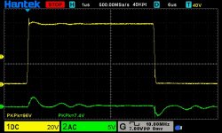
then moved to 50us pulse for 440A, here things get more interesting, Vds switch time is kinda sharp 50ns, at turn on the Vds as it drops down has a step on it in the miller plateau, but the Vgs instead of staying constant it shuts up rings a bit then drops down as previous the shot, the more odd thing is at turn off the Vgs drops nice and after miller clamp kicks in at 2v there is some crazy ringing, Vds goes up over shuts a bit then those ringings as in the Vgs, i don't know what to make of that, maybe is source inductance that rings and is seen on both Vgs Vds...
the 440A Vds Vgs shots
dso_01_01_00_51_24.jpg
dso_01_01_00_51_45.jpg

then chaged the Rgate 4.7R for Ton and Toff, and did 50us pulse for 440A, here the Vds switch time increased to 100ns and the ringing amplitude settled down a bit, but same behavior as before
the 440A Rg4,7R, Vds Vgs shots
dso_01_01_00_38_50.jpg
dso_01_01_00_41_24.jpg
dso_01_01_00_40_19.jpg
dso_01_01_00_39_18.jpg

then did a 5us pulse for low current (about25A) to see is the ringing goes away, it shure did, but the turn on has the same odd drop...
Vgs shots
dso_01_01_01_24_41.jpg
dso_01_01_01_24_22.jpg

then moved to 100us pulse for 850A, here things get way crazy ringing, the desat did not trigger,i have to lower zenner voltage but i'l get to that after i sort tings out with ringing, the strange thing is that ringing occurs on gate just after Vgs gets to 2v and miller clamp kicks in
850A Vgs Vds shots
dso_01_01_01_36_54.jpg
dso_01_01_01_39_10.jpg
dso_01_01_01_39_35.jpg
dso_01_01_01_47_17.jpg
dso_01_01_01_48_29.jpg

I tryed 10nf on gate placed between 1r and 4,7r resistors but made ringing way worst and longer lasting.
I did the 850A sevral times so it does survive that curent, i would like to go up to 1000A for just testing purpose, and to have confidence in the controller that it can handle A LOT of current, and from there down rate for a safe all day long 300A as nedded.
So 2 things i need to sort out: why is that dip in Vgs at turn on and why is that ringing after the turn off on Vgs.
Please fell free to show your thoughts on what i presented here.
 
Can you show exactly how you're taking these measurements?

Switch node looks pretty good for 850A, there's some ringing but it's all over within a short time.

The gates... It's really strange that there's more ringing on the gates than the switch node. Is it perhaps possible that this is being caused by probing?

The other thought i have is whether you've accidentally got a "large" (single nF) amount of capacitance across the isolation barrier.
 
i'm back with more shots, this time i tried 10ohm gate resistors, it did not like it at all, there was tons of ringing on the gates, then decided to go at the other end of spectrum, and went with 1 ohm gate resistor, the switching is "zapping" fast and the surprise is the ringing on gates diminished a lot, here are the shots for 440A pulse test (green Vgs, yellow Vds)
dso_01_01_03_01_27.jpg
dso_01_01_03_05_06.jpg
dso_01_01_03_02_18.jpg
dso_01_01_03_06_26.jpg
dso_01_01_03_04_25.jpg

here is the probing, the probes are with short ground and are jammed between the cut FET legs, the one with white isolator is used for Vds, the other one for Vgs (greater disteance between G and S legs)
if a let the probe connected with only the ground on the S leg and do the test it does not pick any thing above 100mV
IMG_20220516_123651.jpg
IMG_20220516_123734.jpg

so my concluson after this last test with 1ohm Rg , is that these fet-s do not like being switched slow...., and there is something strange on the source, that after the miller clamp kicks in it couples in to the gate measurement... because i can not see (measure) any ringing any where in the gate drive circuit (at turn off), except on Fet GS legs after the miller clamp kicks in
I'l try an 850A test with 1ohm Rg and see how that does...

response to mxlemming post :oops:
O, and one more thing, i just had an aha moment now when writing the post and looking at the pictures with the probing, the probe sits right on top of the negative bus plate, and the 10mm gnd lead sits at 4mm right on top of the bus plate that goes to the Fet leg, could that be what couples that ringing on the gate measurement? most probably, with such high dI/dt on that bus plate :oops:
 
Back
Top