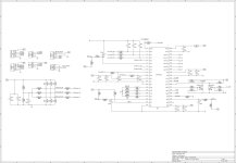
The snubber are between the drain and source.
To chose snubber component values I follow the following cookbook:
- As you can see in your picturs, there's ringing on the drain/source voltage of the FET. Measure the frequency of the ringing.
- Experiment by placing different values of capacitors across the drain / source. Determine the capacitor value for which the
frequency of the ringing is about half to one-third of the original ringing frequecy. This gives you the capacitor value for
the snubber. For a 4115 I found 3.3 to 4.7 nF a good fit (depends on battery voltage, more voltage -> lower cap).
- calculate the impedance of the capacitor at the new (lower) ringing frequecy using X = 1 / (2 * pi * f_new_ring * C_snub)
- the snubber resistor should be taken as 1.5 times the capacitor impedance X.
Now the only thing to watch out for is the power dissipated in the snubber resistor. This is given by:
P_snub_r = f_pwm * C_snub * (V_bat)^2
First put snubbers between all drain/sources of the FET's (see also attached picture where the snubbers are the 4.7 nF and 6.8 Ohm components)
After this is done, look at the gate / source signals. Chose the gate resistors such that there's no significant overshoot which can
blow the gate oxide. Im my controller I didn't need gate resistors, the gate signals looked nice and clean after snubbing the drain/source's.
If the drain/sources are not snubbed the ringing will 'transfer' to the gate by means of the Cgd, this is what you're seeing.