Open Source 1.5-2Kw Charger design

heathyoung

100 kW
Joined
May 27, 2009
Messages
1,545
Location
Newcastle, Australia
Important - this is an unisolated buck topology - the output floats at 1/2 rectified mains potential! Do not come into contact with the battery pack while it is being charged, or the output leads of the charger when it is on. You have been warned!

History:A year or so back I bought a brand new vectrix with a dead charger, no batteries and a dead motor controller.
I repaired the motor controller, and have fitted it with Lithium batteries, but the cheap and nasty BMS battery chargers I have been using to charge it with have a nasty habit of turning themselves inside out on a fairly regular basis - they are poorly designed, and no amount of fixing them will resolve their isues.

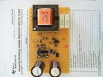
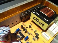
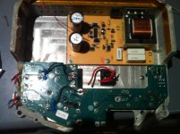
The original charger was a full-bridge, with PFC and all sorts of extra complexity, that defied my attempts to repair it (took full PFC output voltage (some 400V) across components designed for 5V) - so using that was out of the question. It did have some nice bits (including a very nice cast aluminium chassis) and custom wound inductors for the PFC and output filter, along with some nice low ESR electrolytics, and an input/output CMRR choke section designed to handle bulk current.

I came across the DIYElectricCar charger using large IGBT's and chokes in an unisolated buck configuration (not a big deal when EV packs are isolated from chassis) but the size was too large (needed 1.5-2Kw vs 10Kw) and the use of microcontrollers in a power supply - don't like it. They have their place, but this isn't it.

So I designed my own - I wrote a useful excel calculator for determining the correct frequency for the inductor I was using, and using the TL494 design guide written by TI (note - there are numerous errors in this!), along with the design guidelines for the IR2125 high-side driver.

Since this is designed to be completely open-source, I will publish the schematics and all of the information, I split the schematics for clarity.

Design:
My design goals were:

Constant Current (0-12A)
Constant Voltage (0-150V)
BMS Control with soft-start resume
Inrush current limiting with Bypass (important - thermal inertia of the NTC thermo and power wastage is a concern!)
Robust drive section that can handle abuse and cycle-by-cycle current limiting to protect devices.
DC input capable for dump charging from a Sealed Lead Acid bank


With the exception of the last item, a good charger (such as the Elcon) would fit the bill nicely, but a $600 pricetag, and the fact it doesn't fit anywhere nicely on the bike kills that idea!

Control section - this is based on a TL494, running as a single ended configuration at 100khz. The first opamp buffers the output from the voltage divider (no real reason apart from that there was a spare one, and it limits the output to the bias rail if something goes bad) the second amplifies the shunt output by 10X. The two pots control the V and A limits. The BMS input sits across the soft start section, which ramps the output over 10 cycles. When the BMS gets triggered, the TL494 stops pulse output to the IGBT driver, and soft-starts when it is removed.

View attachment Control_Section.pdf
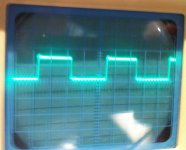
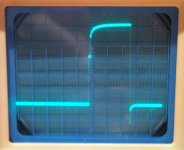
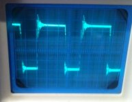
TL494_Output.jpg

Inrush current limiting - Very simple, basically a 3 second delay circuit when the power is applied - this drives a relay to close across an NTC thermister in series with the bridge rectifier that charges the resovoir caps - The low ESR 1500uF @ 360V bank draws a LOT of current, so a very robust NTC is required, anything smaller actually explodes on start-up (ask me how I know that). During startup, the only thing the NTC needs to be doing is charging the caps - not supporting the load of the charger, so there is an additional relay that sits across the soft start circuit so the charger only starts to produce output when the soft-starter is done.

View attachment Soft_Start.pdf

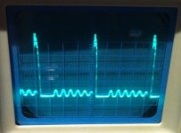
Drive section - this is based on an IR2125 set up for current limiting - there is a fast recovery diode across the resistor to speed up the discharge of the gate, bypassing the resistor and allowing the gate to discharge FAST. The effects on the gate drive are very noticible in the scope traces, reduces the amount of time the IGBT is not saturated. The 7555 timer provides extra boostrap voltage for very high and very low duty cycles. The shunt resistor on the drive section provides cycle-by-cycle current limiting to protect the IGBT if something goes bad. The IGBT and recovery diodes are heavily over-specced for robustness, 2Kw is very possible with these components. The choke is a custom job from the output filter of a Vectrix charger, but high power chokes are readily available.

View attachment 5
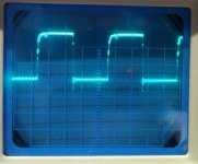
Gate_Drive_Post_Diode.jpg
Gate_Waveform_Single_Pulse.jpg

View attachment Driver_Section.pdf
 
Testing today.

Some revisions and lessons.

1) Don't bother amplifying a shunt voltage - all you do is amplify a shit load of switching noise and build a great musical instrument. Squeals, chirps - you name it.

2) Don't bother buffering a voltage divider - all you do is slow down the feedback loop and make the PSU angry.

3) Half-assed attempts at current limiters (like using voltage comparators, or slow opamps) screws BADLY with the feedback loop - I have very little loop compensation so this may be the issue.

4) Proper current limiting (on the scope) looks like foldback voltage adjustment - if it jitters or squeals - it isn't stable, and you are beating the shit out of components. The IGBT I am using is damn near indestructable - I deliberately shorted the supply and it just protected itself. No bangs, no pops - nothing. Pull the short off and put on a load and it bounces right back.

5) 150VDC HURTS! :evil: Put drain resistors across the damn caps!!!

Results (after quite a few modifications) - Adjustable current limit from 0 to 15A, adjustable from 0-120V (with 150VDC input) so 0-300V with 240V AC input.

At very low duty cycles, gets audible since the TL494 'jitters' at extremely low duty cycles - I think it is dropping pulses. Under hard current limiting (like a large bank of paralleled dichroic halogens) it gets quite vocal (sings at about 10-12Khz).

With the massive heatsink of the charger - no real heat evolved at low power levels (600W) - will be trying for 1.2Kw tomorrow, and 2.4Kw if I feel like testing it that hard.
 
Bump,

First - great idea and needed... Considering the number of blown primary transformers available from blown chargers, this could be a great way to build new, compact 1.5kw chargers and Open Source is the way !!!

So far the design looks good, after reviewing dozens of USA and Chinese chargers I've found their flaws.

Keeping it fully analog is great, it does cause some whine as you found at lower voltages because of the 494 but eh...

May I ask will you be sharing your schematics, PCB CAM Files (Gerbers, etc) or have an Open Source site setup yet..... perhaps a BOM.

I'm in the states - personally I'd rather build my own 1.5kw chargers for my rides, then I know what's in them, dissipation ability - deration to 1000w for handling poorly powered 110 AC outlets, etc.

Your contribution is appreciated !

Thanks!

-Mike
 
I've got to modify the schematics, I made quite a few changes to the control section, based on today's test run.

The PCB files I will post up - they are express pcb (free software) so easily modified / updated for your own usage. I should use something like protel but CBF :mrgreen:

Interesting idea with recycling the transformers from a forward converter - I actually recycled the filter transformer (which was wound on an etd core - with copper foil and I haven't managed to even get it warm yet, so its hideously over-specced like the rest of the design.) There were three usable chokes - the forward converter transformer, the PFC transformer and the Filter transformer - I used the filter transformer due to the inductance and construction method.
 
Well, 2.4Kw was a bit too much for it unfortunatly.

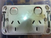
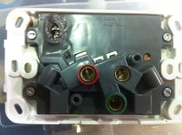
Casualties were - two IGBT's (shorted across all pins), a kettle and a powerpoint. Sigh.

Lessons - Excessive DvDt is bad - what looks like a nice trace on a scope at lower voltages probably results in massive negative-going spikes that exceed VGE. Since there is no protection from this, I'd say that this results in the device lockup and subsequent destruction.

At least with this topology, when you short a device its not a spectacular explosion.

Don't use AC switches for DC!!!

Back to the drawing board... sigh. :|

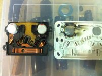
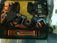
This was a powerpoint rated for 240VAC 10A passing (and subseqently trying to interrupt ~320 VDC @ 12A)

Front.JPG
Rear.JPG
Open.JPG
Welded.JPG
 
Thoughts - might be a good idea to slow the switch-off down - the diode on the gate drive is probably way too fast and is causing massive headaches.

Off to the local electronics shop for some Transzorbs - 400V 1.5Kw should od the trick nicely, if I get these to explode, I at least know what the issue is. The gate drive needs to be slowed down and protected.

There isn't excessive current, and there is no thermal issues, so I bet I am exceeding VGE (+/-20V) or VCE (1200v eek!)
 
After more thought - the transorbs are treating the symptoms, but not the cause.

The noise under load from the inductor is excessive, leading me to think that there is some instability in the feedback loop - I have the loop gain set a the standard TL494 gain of 1000 - its unstable at low duty cycles, which I think is causing the IGBT to get beaten up badly. Setting the gain lower (to 100 or so) may improve this situation.

What works perfectly at DC gets lost in a sea of noise at high currents. Time to rethink the board design too I think.
 
I replaced the IGBT (again) and put a 15V bi-directional transzorb between Gate and Emitter, and put a low (120W) load across it and scoped the gate drive - holy mother of... there is a pulse in there somewhere! Could hear the choke hissing - its uuugly. On the plus side, the voltage regulation was excellent - 150.0V was held regardless of the input voltage, as long as it was over 160VDc on the caps.

Definitly a board redesign is in order - probably need a star point grounding or ground plane design. I'd prefer not to go ground plane for the danger factor when adjusting voltages etc - the 'ground' plane sits at lethal voltages - not good.

I'm looking at alternative control schemes, such as Hysteric buck - there is a nice LED driver IC that requires minimal components, and is current mode control, with an over-voltage cutoff, high side and low-side mosfet gate drive (and synchronous control if needed) - its an IRS2541, the only problem is that it needs to drive a low gate charge Mosfet - 25nC or less, I have narrowed it down to some parts with 33nC gate requirements, will see how they go.

Another contender - more what I was after - FL7701M, Buck, PFC(!), analog dimming, pulse-by-pulse limiting, soft-start, IGBT/Mosfet driver ~ woah. $5 in quantity.

Gate_Hash.JPG

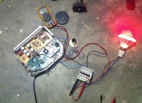
Test_Rig.JPG
 
do you have circuit schematic so we have an idea of what you are doing? none of the terms you use rings a bell/or why you make it this way. is it just because it makes power without so many components that is the reason? but the power is usable by the battery because of it's capacitance? so that the noise is a non factor, except for the euro EMI regulations?
 
Schematics are in the top post - I need to update them, quite a few changes.

The topology is unisolated buck, uses a TL494 as a 100Hkz oscillator, driving an IGBT through an IGBT driver. The noise on the gate drive is destructive - its been responsible for the demise of two IGBT's so far, so it is far from ideal! Output voltage is rock steady, but the triggering is extremely hit and miss. The batteries don't care, they are basically ideal RC circuits with extremely long time constants.

I think I am getting false triggering all over the place, and need to redesign the circuit board - star point earthing is where everything is earthed at one point (ie. the centre of the star) and radiates outwards - the current layout I would have all sorts of strange earth loops going on. The board design was a quick and dirty I did ages ago, its the first revision, so won't stay like this.

The other way to do this is to use a ground plane design - double sided board - with one side for the tracks, and the other for ground return - commonly used in RF and video bandwidth circuits - its a brute force approach to noise control, but I am getting pissed off with frying components.
 
I revisited the design of the PCB - there is a LOT more copper on there now, thanks to the fill command, creates a ground plane, so hopefully this will resolve the issues with the tracks being highly inductive.

The creepage distances are 2.5mm, in line with UL regs.

Also removed for testing purposes the 7555 derived bootstrap for the IR2125, and will rely on the boostrap cap only.

I'm buying some more PCB boards to make this newer version, hopefully I have some more success with these modifications.

Not shown are the multiple (10) SMD 1812 package MLCC 0.1uf 500V ceramics scattered across the rails.

There is also now 6 X 330uf 450V low esr caps on the rails (!). A very large thermister needs to be used, the pansy little things that come on (even the larger) BMS battery chargers actually explode with the inrush current on this. You end up with two legs and a heap of soot on a PC board - moderatly amusing.

Mental note - make sure the charger is not producing output whilst in pre-charge - at 2Kw there was rather a disturbing amount of smoke rising from the thermister!

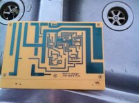
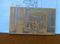
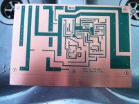
Older version - those thin tracks did carry the current, but with an unbelieveable amount of inductance at 100Khz @ 10A

View attachment OLD_Design.pdf

Newer version - designed for rather a lot of current and very low trace inductance.

View attachment New_PCB_Design_Ground_Fill.pdf
 
Well, another update.

I have now got the circuit running nicely - but I'm still killing IGBT's dagnammit.

The updated PCB made diddly squat difference to the instability problems - what fixed it and made it completly stable was increasing the output capacitor, and putting a 0.1uF ceramic between pin 2 and pin 3 (voltage comparator input and compensation pin). The current feedback required a considerably larger capacitor (10uf!) to make this loop completly stable. Voltage is adjustable from 0-90% duty cycle, and current is adjustable from aboutr 5%-90% duty cycle.

OK - I seem to be having some fun and games when the circuit starts - an audible clack is heard from the inductor - this would be the inrush current into the output filter cap, for some reason, it isn't being held back (probably due to slowing down the current feedback loop). Inrush current is manageable with 120V DC, but at 320V DC, that current spike is lethal to the 25A IGBT.

So - options. Fix the bloody current loop. Use the one comparator rather than two. Put an IGBT with some serious testicular fortitude into service (eg. FGL60N100BNTD - 60A 1000V), fit snubbers across it, fit transzorbs on it.

I've now toasted my stock of 25A IGBTs and I don't think I will go back to that model (don't like the to-283 package)
 
I've made some more progress.

I've realised that the reason for the large current spike was that the soft start cap was too small, the feedback loop too slow and the output cap too large. Due to the topology, the output must be loaded for the boostrap cap to charge, and the IR2125 to produce gate pulses. Starting the power supply, and then applying load afterwards results in the TL494 running at full duty cycle, so the first pulse that hits the gate is at full tilt, so it beats the snot out of the IGBT before the current limiting has a chance to respond and wind back the duty cycle.

So - I have increased the soft-start to 100uf (from 10uf), made some changes to the compensation network (added resistors to make a constant input impedence to the error amplifiers - the variable resistors wer changing the poles on the bode plots, making stability almost impossible to achieve - this is why you have problems running a SMPS out of its designed voltage range - the compensation network gets messed up, and the supply ends up unstable).

What happens now is that the precharge delay also runs another relay across the 'BMS' terminals (DTC soft start circuitry) so when the precharge has happened, the TL494 slowly ramps up its output with adequate time for the feedback loop to stabilise. No squeals, chirps or thunks from the inductor now, unless you turn off the load and reapply it (bad idea). Then the problems begin.

Soooo.... When it is used as intended, it works well. Drop the load and bad things happen. The protection circuitry on the IR2125 needs to be enabled prior to the load drop (i've got it disabled at the moment) and potentially the protection output should go to the dead time control pin somehow. This would stop the 'motorboating' when the protection hits (it pulses the output, and at full duty cycle into the inductor, it isn't nice.)

More design work needed, but a lot more positive than before!
 
I can;t help at all... but I'm watching closely and hopeful I could build one for my bike some day :)
 
knighty said:
I can;t help at all... but I'm watching closely and hopeful I could build one for my bike some day :)

Ditto : )
 
Thanks for that - I have resolved the issue with the IR2125 - it appears that the Vcc rail was dipping below zero, placing a diode in series seems to have resolved this. This means that the current protection of the IR2125 is now fully operational, and I might not be responsible for the death of another IGBT (hah! :mrgreen: )

This weekend I am planning to do another full power test, ramping up to 1.5Kw, but not trying to drop the load on it (since it kills things).

The ultimate goal with this design is to probably move from a buck topology to a half-bridge. I'm getting togther the parts for a 2Kw half-bridge, fully isolated version, using an ETD59 core, 100Khz and Litz wire (rather than foil winding - due to the skin effect at higher frequencies, solid windings are a no-no).

Full-bridge is probably a better idea for power density, but I need to stop making things go bang first :) Ideally a PFC version is also in the works.
 
Results - yet another IGBT death. Was happily charging away at 150V 5A, and I pushed it further, and blew out another one.

I also discovered that you need to have a load on the supply - It won't charge without it - 10mA is fine. This also resolves the removal and application of the load issue that was killing it before.

I'm starting to think that these are counterfeit components - every time I push these I seem to blow the bloody things up with little provocation.

They seem OK - but I don't think they are real. Whenever I push them over 12A, they die. They are 25A components.

The other possibility is I am pushing it out out of its SOAR (safe operating area region) - Very fast pulses require some de-rating of the IGBT.

Time to stop ordering components from Ebay! :twisted: Farkenell it is - funny thing, the component I am after is the same price from Farnell as Ebay.
 
EXCITING NEWS!

I swapped out the Chinese crap that was masquerading as a genuine Fairchild IGBT, and threw in a known genuine, brand new IRFP460 MOSFET (I added a 10K resistor from Gate to Source, and a 400V 1500W transorb between Drain and Source in leau of a snubber network.

Well, damn me if the thing is now indestructible! I put it through some awful testing (400W of halogen Dichros - switched on and off at 0.5 Hz, the current limiting did its thing and nothing happened, it accepted the load with no mess, no fuss!

I even like the package (TO-247) as it heatsinks well and is easily isolated from the chassis.

Next is the PSU's nemesis - the kettle of doom!
 
Testing!

The unit is silent until 155ish volts (ie. 50% duty cycle), then it starts to make noise - its pretty quiet compared to the noise of the kettle. Seems to be the current loop rather than the voltage loop that is the culprit for the noise.

The Mosfet finally gave way at 190v with a 24.1 ohm load (7.88A, and 1497W) Booo! Didn't even make it to 1.5Kw. All you hear is a tiny little 'ping' from the inductor, and the output goes unregulated.

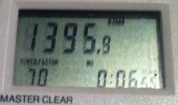
Power factor is 0.7 at these loads, which is acceptable for a non-pfc supply.

I'm reasonably happy with this result, needs more work obviously, but a 1.3Kw stable output is pretty nice.

Tried again, killed it at 190(ish) volts (1.5Kw), so this seems to be the limit for this Mosfet. You get that. Might have another look at beefier IGBT's vs the Mosfet, will be buying genuine parts this time, I've learnt my lesson about buying parts from Fleabay.
 
Subscribed
 
looking good

planning 60ah hours on my new bike so need a high output charger for it !
 
Some photos...

Light load - 48V @ 3A
Light_Load.jpg

Heavy load - 48V @ 12A

Heavy_Load.jpg

Power factor - Mains input voltage 247V, resistive (kettle) load

Power_Factor.jpg

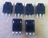
Casualties of war 4 X Ebay IGBT's, all failed at under 600W (Supposed to be 1200V 25A). 2 Genuine IRFP460's failed at ~1.5Kw.

Casualties.jpg
 
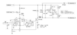
I'm having a major rethink about voltage mode regulation - I have decided to move from voltage mode to current-mode regulation.

If one is to take a buck converter and re-arrange the components, it is possible to have a low-side switch - this is a great thing, especially since you can use cheaper low side drivers (or even better - utilise a cheap current-mode IC with a totem pole driver, such as the UCC3804) This cuts the component count considerably, and also drops the cost - a UCC3802/4 is only $3, whereas an IR2125 is $12!

It also has the massive advantange of pulse-by-pulse current limiting. You can short the output, and the current across the mosfet is limited. No more blown IGBTS or Mosfets - the peak currents never are allowed to get too high.

The UCC3804 is also duty-cycle limited to 50% - so output voltage cannot get any higher than 1/2 rectified mains potential - in my case, this is 170V, the charger only needs to be 160V. This also simplifies compensation, as only the voltage loop requires compensation, not the current loop (which was proving to be a MAJOR PITA for the voltage mode design).

I have attached a preliminary schematic (subject to change of course) showing how simple this solution is.

Current_Mode.jpg
 
Back
Top