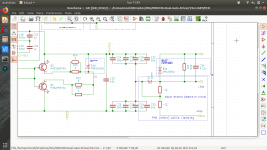
OSHW TO247 IGBT watercooled laminated half-bridge

Hi all,

Concerning active clamping against Overvoltage at Vce when fast Turn off of IGBT gate, I found those interesting docs which shows two different approach that seems to be superior to the active clamping listed above:

Advanced active clamping :
http://www.power-mag.com/pdf/feature_pdf/1260811353_CT-Concept_PEE_0809.pdf

Dynamic active clamping:
https://www.infineon.com/dgdl/Infineon-PCIM_2008_Robustness_improvement-ED-v1.0-en.pdf?fileId=db3a30431a5c32f2011a5dee3e7900b2

What do you think is the best approach between them?
 
Thanks for the input

AAC is implemented at asic level by the company that developed it so even though I have seen the whitepaper and I have here an AAC enabled driver, I'm not confident I can get such circuit working.

About dynamic active clamping, adding a capacitor to set the timing of critical mechanisms is stuff of nightmares to me. I dont know enough to get involved into that right now, and I've seen those approaches only in higher voltage applications like >3kv switches or multilevel topologies. Maybe its not common practice at our 500-ish volts? If I can test it and it works better for sure I'll implement it, its adding 1 cap.
 
Yeah, all this active clamping stuff is a bit confusing for me...

Even the company you are mentioning has ditched AAC in their new ASIC IC from what I understand...

Take a look at their newest ASIC chips for sub 110kw design:
https://gate-driver.power.com/products/scale-idriver-ic-family/

Those ASIC chips seems to simplify the gate driver design a bit...8 amp output is enough for sub 110kW applications which is a nice feature I think. Does not seem to have more than Desat protection function which they call differently. Very similar to ISO5852 but cheaper and higher 8 amps output so you can simplify the circuit by removing the amplifier level in the gate driver...
 
Um, thats a cool IC. Can you order those from common suppliers?
The only thing I can see is worse than the TI chip is the common mode immunity, from the datasheet it makes it not suitable for driving SiC mosfets, and the ISO5852 is.
They have a good reputation, I'd trust that driver.
 
Great catch, thanks for sharing. Its worth a try I think.
 
looks like a decent chip if its <$6. but don't follow their layout advice, yikes :shock:

also, i don't know why they call it active soft shut down.. its basically not much different than your two-step turn off. other chips do this just as well. and there is no transient voltage protection here which is fine cause it shouldn't be needed at the power level this chip is made for. i'm just pointing this out because very fast now that decent systems are working we will see the desire to go to ultra high power (@arlin) and this chip is not good enough for that.

use this chip for applications <50kW continuous rated and should be OK. some time ago this company was known as IGBT-Concept and they were great. i'm assuming the same people back then are still working for power integrations so hopefully they still designing great stuff
 
HighHopes said:
(@arlin) and this chip is not good enough for that.
for applications <50kW continuous rated and should be OK.


Yeah I was thinking about how people look for a cheaper drive chip... Mine are like $20 each.... But when the 3 driver boards cost ~ $1000 to build up Saving $84 for all the hassle and work involved in redesigning my driver boards is not appealing. Not to mention the potential for fires and more failed $300 IGBTs which commonly fail in pairs...

I think I look at price when I look at components but with the driver its down the list...
 
Concerning gate driver overshoot protection ... again :lol:

Does someones knows about this active clamping technique from TM4?

https://www.tm4.com/wp-content/uploads/2014/03/ATZelektronik_05_2012_scientific_article_TM4_power_electronics.pdf

It seems that it might be difficult to make it work properly (it needs manual adjustment), but maybe it works well when done properly... The technique is indeed easy to implement on the hardware side (but might be costly to test if it does not work at the first try because of bad resistor values)
 
ENNOID said:
Concerning gate driver overshoot protection ... again :lol:

Does someones knows about this active clamping technique from TM4?

https://www.tm4.com/wp-content/uploads/2014/03/ATZelektronik_05_2012_scientific_article_TM4_power_electronics.pdf

It seems that it might be difficult to make it work properly (it needs manual adjustment), but maybe it works well when done properly... The technique is indeed easy to implement on the hardware side (but might be costly to test if it does not work at the first try because of bad resistor values)

It's the 1st time I see someone else mentioning that technique :D (di/dt switching current limiting through source stray inductance). I unintentionally did that in a controller, when I knew less, and later when I analyzed my PCB to understand why it didn't make huge spikes I concluded it was because it had relevant source stray inductance. I have explored the concept a bit under simulation, and there's a sweet spot for the inductance value for each case. The inductance acts as negative feedback wrt the driver, controlling di/dt (and therefore spikes). I think I've mentioned this somewhere, even maybe using ampops to synchronize paralleled power switches and ensure "equal" current sharing.
Thanks for the link!
 
Another effect I initially noticed on my controller that didn't seem to make sense was that the FET switching speed was not increasing after a certain point while reducing the gate resistor. That's because of the negative feedback with the stray source inductance, which "clamps" di/dt.
 
Well ... I could add this on my to do list for my next version of my homemade "dual gate driver" (V0.3)... it is only adding one resistors and a separate connector that connect on the power bus...
 
This is interesting.
 
It looks impossible to achieve if you have several parallel devices, however its doable if you are using a module. I would like to have a picture of their setup so I can see which point they choose to increase the stray inductance. If that loop is too large it will become susceptible to EMI, and its the gate trace what we're talking about here.

One thing to consider, they use a parasitic element (L) of the module. What happens if the manufacturer improves that inductance without telling you? Your protection would be less effective, should you test every powerstage you build?

Me personally, I'd stick with active gate clamping with a zener. It is triggered by the direct cause of failure (Vce) and doesn't rely on parasitics to achieve protection.
 
Asking for pictures too! If someone somewhere has a TM4 drive :D

In what you are saying Marcos, there is a lot of facts, but also some suppositions without equations/simulations. That's why I'm asking

I have also read that clamping with a zener is not always 100% functional, but it is more straightforward this way i agree.
 
Oh sure. I just remember HighHopes telling me to NOT use even a testpoint in the gate driver trace. I imagine his face transforming when I tell him I'm about to connect a inductance to the gate trace :p
 
In the controller I mentioned I have it in the DC link caps - low FET source. When I talked about this in another thread, HH just said above 10KW you don't want to add any source inductance.
 
There is no need for any additionnal inductance according to the doc that I have posted... it is using the emitter connection from the igbt and a second connection a bit outside of the igbt on the dc- bus when on the low side igbt or a connection on the phase busbar when on the high side...the small distance between the two connections generate enough voltage drop during high current igbt turn off to shoot back emf voltage on the gate automatically...you use a voltage divider between the two emitter connections and the gate to limit this voltage to an acceptable value for limiting Vce and Vg

all drives from tm4 are using this tech according to their website... tm4 are building motor and drives for 30years now and have manufacturing agreement with several o&m manufacturer. I guess their tech is functionnal. they use only infineon modules in their drives apparently.
 
maybe what you wrote was unclear to me...


if you mean that the small circuit connected to the resistor divider and gate driver would add unwanted parasitic inductance or antenna lossses to the gate circuit...that would be incredibly small i think if you take care of the circuit.
 
sorry I wrote that of a really unclear and false way:

you use a voltage divider between the two emitter connections and the gate to limit this voltage to an acceptable value for limiting Vce and Vg

Let's start over :
During fast turn off at high current, you use the voltage created between the two differents emitter connections(the one on the module & the one on the high power circuit) are used to raise the reference voltage, so Vge become suddently higher (The diode block the difference)

The final circuit would be like this i think:

TM4 reflex circuit.png

but anyway, that's complicated stuff I agree...I will give up on that for now :lol:
 
Back
Top