DIY 6FET Controller help

that's the best double pulse tester i ever seen!

300mv droop on driver output is nothing. but the chip is only rated for so much current so that you must be careful for. if you need more current you need boost stage or different IC.

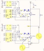
can you post a schematic of your test and where the probes are with respect to the schematic.

are you using differential probe? if you are using regular probe, that's probably the reason for the ringing

be careful for your double pulse setup, it should not allow more than 2 pulses. this is because you might actually be testing a drive where the desat does not work or has wrong threshold or you have some other weakness revealed. it would be nice if your only had 2 pulses allowed into a bad scenario instead of an infinite run which could actually cause big problem.
 
SjwNz said:
Finally made my self a Double Pulse Generator, Pulse 1 - 3 to 999uS . the interval and Pulse 2 have the same pulse widths and
range from 3 to 100uS with a option to turn off the 2nd pulse. Also added a input for Desat to disable pulses if DaSat is triggered.

View attachment 4

So I setup the controller with my battery(46V) a 10uH coil connected to +Bus and Phase C. Setup the scope to look at the LowSide FET and Phase C.
Increased Pulse 1 width until I got around 30uS was gave me a current of 150Amps with Interval and Pulse2 set to 5uS.
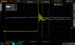
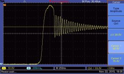
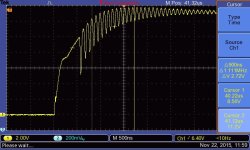
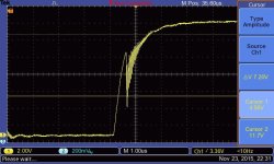
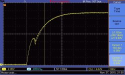
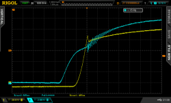
Now this is were I got messed up Ringing on the 2nd pulse on the Gate
Yellow Trace = GATE Blue = Phase

View attachment 2

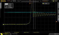
I was thinking it was common mode noise, so did the (Short the probe to its ground clip) and
placed on Source of Low Fet and only got a signal around 200mV which to me did not seem that bad? Then today I was able to
borrow a differential probe and did the same test and the result had less ringing but the same spike so I am mostly happy
all this ringing from the gate is not common mode noise based on the small amount of noise I measured.
View attachment 3

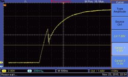
So I played around adding more Sunbber caps to the bus which did nothing, My turn on time was slow at 3uS with the 40ohm ON resistor, I lowered the Turn on Resistor value to 15ohms and did not make any difference but at lease I got the turn on faster to 1uS.
I then added 50nF cap across the G-S, maybe not the best for the gate driver but greatly reduce the ringing.
Yellow Trace = GATE Blue = Phase
View attachment 1

I started to look at the Phase and Gate and noticed when the Gate was been turned on which causes the Phase voltage to drop to -Bus
when the Phase voltage reached around 12V which is the same voltage as the gate, it started to pull the gate down due to miller effect, which turn the fet off, Phase Voltage would start to rise and gate would recover and FET turns on again doing this over and over until it stabilized. Going over this now is just basic MOSFET miller effect stuff but took me a day to think about what was happening.
Yellow Trace = GATE Blue = Phase


So it makes me think my gate section has to much inductance due to crap layout or the Gate resistor I am using are rubbish.
Very nice. Having a desat input is a great thing. Does it tell the user if desat was triggered?
 
Made a Boost stage from a TIP41 and 42 transistors and using 10ohm ON, 5ohm OFF and no difference to the ring.

HighHopes wrote:
can you post a schematic of your test and where the probes are with respect to the schematic.
Gate & Phase measurment points.jpg


HighHopes wrote:
are you using differential probe? if you are using regular probe, that's probably the reason for the ringing
Yes I am, but when I connected the Diff probe ends together and placed it on the Source of the LowFet I can still see 200mV of CommonMode noise.
its almost the same amount as standard probes.


be careful for your double pulse setup, it should not allow more than 2 pulses. this is because you might actually be testing a drive where the desat does not work or has wrong threshold or you have some other weakness revealed. it would be nice if your only had 2 pulses allowed into a bad scenario instead of an infinite run which could actually cause big problem.
It will only send out 2 pulses, if you hold down the GO button it will send the 2 pulses then times out for 2sec


Arlo1 wrote:
Very nice. Having a desat input is a great thing. Does it tell the user if desat was triggered?
When DESAT is detected it will disable the pulse and then tell you if Desat happened in the 1st or 2nd pulse.


Just did some more testing again but on the HiSide fet, Coil now connected from Phase to -BUS, and got the same ringing on the HiSide fets gate. Added a G-S cap and reduced ringing. Not sure if this is useful but the ringing is always 22MHz , with or without the G-S cap.
 
22MHz is pretty high, its like a resonance. it might not be real, or it might be real but only appear when you connect your probe (your probe has capaccitance after all). this is hard to explain how to resolve this confusion, but i get the sense you are not new to electronics so probably you know of this already.

remove your mosfet and put a capacitor there instead. cap value to be about the same as your effective gate capacitance. the cap is placed gate to source. this is tested without the double pulse setup, here you are just charing and discharging a cap.. looking for clean switching. if not clean then you know problem not in the mosfet or noise coupling through mosfet to your gate drive. you are looking for some sort of PIE network resonance.

another test you can do, carefully and only if you understand what i'm about to say, remove the isolation of the lower gate drive and tie digital ground to power ground. so your opto still works is just not isolated. your power supply for that gate driver i think it doesn't matter if you do the same. tie power ground (i.e. mosfet source) to digital ground by soldering a wire. this is ONLY for the lower gate drive. now you can use your regular probe on the lower gate/source and you can clip your prove ground pin right to the mosfet source pin. this should be the ONLY ground purposely connected between scope and board. do not use two probes. well, you can use two probes so long as the other is diff probe, but don't do that for not make sure you using only one probe to limit possible source of problems.

you get the same crappy waveform on all gate drivers? hopefully yes so you know it is more likely a design problem or a measurement problem.

your schematicc is perfect, i just like to double check. looks like Protel :)
oh, i was wondeirng about yoru DC link cap. you show 0.33 but i think this is your snubber. you DO have large DC link cap right? and it is physically located very close your mosfet phase leg, not far away in your double pulse test box or something. i know.. stupid question...
 
The 22MHz can be resonance between the MOSFET Coss and the trace inductance (incl. MOSFET pin). To test it you can add 1nF capacitors between the drain and source of both the high and low MOSFETs, and see if the frequency is lower.
 
remove your mosfet and put a capacitor there instead. cap value to be about the same as your effective gate capacitance. the cap is placed gate to source. this is tested without the double pulse setup, here you are just charing and discharging a cap.. looking for clean switching. if not clean then you know problem not in the mosfet or noise coupling through mosfet to your gate drive. you are looking for some sort of PIE network resonance.
Not to sure how to workout my mosfets effective gate capacitance yet, I am starting to read papers on this, bit I placed a 50nF cap and wave form was nice
and clean.


another test you can do, carefully and only if you understand what i'm about to say, remove the isolation of the lower gate drive and tie digital ground to power ground. so your opto still works is just not isolated. your power supply for that gate driver i think it doesn't matter if you do the same. tie power ground (i.e. mosfet source) to digital ground by soldering a wire. this is ONLY for the lower gate drive. now you can use your regular probe on the lower gate/source and you can clip your prove ground pin right to the mosfet source pin. this should be the ONLY ground purposely connected between scope and board. do not use two probes. well, you can use two probes so long as the other is diff probe, but don't do that for not make sure you using only one probe to limit possible source of problems.
Only made a very very small difference to the size of the ring.

you get the same crappy waveform on all gate drivers? hopefully yes so you know it is more likely a design problem or a measurement problem.
I forgot to do this, so far the gates from Phase C Hi and Low side have this ringing I will try test the rest tomorrow.


your schematicc is perfect, i just like to double check. looks like Protel :)
You are correct, Autotrax, Protel , DXP , Altium or whatever they call it now :)


oh, i was wondeirng about yoru DC link cap. you show 0.33 but i think this is your snubber. you DO have large DC link cap right? and it is physically located very close your mosfet phase leg, not far away in your double pulse test box or something. i know.. stupid question...
0.33uF is the Snubber and a bunch of 470uF caps for DC-Link caps ,I forgot to put in the Sch . doh


Peters wrote
The 22MHz can be resonance between the MOSFET Coss and the trace inductance (incl. MOSFET pin). To test it you can add 1nF capacitors between the drain and source of both the high and low MOSFETs, and see if the frequency is lower.
ended up using 2nF and that ring Freq changed to 15MHz.


I decided to do a little test and made a 1/2bridge using some double sided PCB as a laminated bus with DC-Link cap & Snubber cap , and same fets I am using in my controller. But this time I used a 4420 Gate driver chip made by MicroChip which is rated at 6amps. I used a single 10ohm gate resistor, connect my double pulse gen and the 9uH coil. Used the same pulse 1 time of 30uS so current should be 150amp, and still got the ringing in the gate .
And like before the ring does not start until gate voltage gets around 8volts.

while I was messing around I replaced the FET doing the switching with one I had laying around for 10years, it was only rated at 20amps but was 500V. I started at 20amps and the ring was there but not that bad, but by the time I got to 150amps the ring was almost gone.
But I was pushing that 20amp fet way to hard so that result maybe a waste time.
 
50nf is huge your gate is 19860pf or 19.8 nf. At the voltage they tested at which is 10 and what voltage are you running to the gate? You have to measure the gate during switching to know this. But anyways a bit of a rule is I try not to add more cap to the gate then the gates capacitance it self.
 
I've been spending a lot of time working on a new layout, a very large parallel layout of 11 TO-247 devices. I've been taking notes on every lab that I have been doing with lots of scope screen shots. I would strongly suggest that you take lab notes as they really help you form a picture. I've found my best notes are taken as I'm going vs summarizing afterwards. One Note from Microsoft is an awesome solution.

Anyways, the reason I came here...

So I wanted to show everyone this neat math trick to help them calculate their approximate layout inductance since it's quite difficult to measure directly. When doing the below test I suggest using a few different values of Cadd and then averaging the results as it's not a perfect method.

Step 1. measure ringing freq
Step 2. add a known capacitance drain - source
Step 3. measure ringing freq again
Step 4. math

f_ring0 = 22MHz
f_ring1 = 15MHz
C_add = 2nF

f_ring = 1/(2pi * sqrt(Llk * Clk))

With some algebra we end up with
Clk = Cadd / (x^2 -1)

x = f_ring0 / f_ring1

1.467 = 22MHz / 15MHz

2nF / (1.467^2 - 1) = 1.736nF <--- this is the about the parasitic capacitance of your layout

Clk = 1.736nF

1/(2*pi*22Mhz)^2 * 1.736nF = 30.2 nH <-- this is about what your parasitic layout inductance is

Llk = 30.2 nH

*When doing any pulse testing with an inductor, make sure it's several feet away from your measurement setup so that the magnetic field does not distort your readings. I moved my inductor about 5' away and placed it on the floor using some 8 gauge jumper cables.

While I am using parallel devices and you are not, most of what I am saying here is applicable. This is the layout I'm working with. I've managed to get the layout inductance <70nH on two of these. With 5 parallel devices I measured 49nH and then with all 11 devices in I measured 69nH. This was designed paying careful attention to layout loop area due to being quite long. If the above numbers hold true (need more testing) then each additional MOSFET in parallel adds 3.33nH of inductance. Working backwards this means the layout by iteself ~32.3nH since 11*3.3nH = 36.6nH. Not too bad considering there is ~170mm of bus length from DC link cap to the last MOSFET. The lower you can get your layout inductance, the less you will have to deal with ringing issues. Minimize loop area everywhere you can!
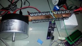
test setup.jpg

I've observed that turn on ringing is significantly reduced as I turn on the devices faster. That is I see more turn on ringing on my double pulse testing with a 1000ns switch time than I do at 500ns. I'm not certain on this observation yet as I have not mentally worked through the MOSFET turn on operation and all it's elements (such as the LC tank circuits it creates) yet as I have with turn off ringing cause / effect. I have also seen that the load inductance will cause the turn on ring to vary in amplitude but not frequency. The amount of bus voltage will also vary the amplitude. I found that higher bus voltage yielded lower ringing amplitude.

For double pulse testing, your total period after the initial charging of the coil should be close to 1/Fsw. If you plan to run the controller at 20kHz, then your off period after charging should be 25us and your 2nd turn on should also be 25us. This is simulating a 20kHz switching interval at 50% duty cycle. I've been using this method to evaluating current sharing between devices and it's been very useful. If you want to see how the device behaves at 10%, then set your off period for 45us and the on period for 5us. Trick is to maintain the total off/on period and just vary the duty.

Here are some screen shots of my double pulse results for comparison. I spent a lot of time figuring out how to minimize any ringing in my layout. If you really want to get good at this it's important to spend a lot of time bench testing and playing around. Simulation is also good for this.

This shot shows the following
Ch1 = Drain - Source
Ch2 = off
Ch3 = total current going through array, 100mV = ~100A
Ch4 = D-S current through device in circuit (I'm using a Rogowski coil)
Math = integration of current in 2nd on period (I'm studying current sharing between devices)

This pic shows a ~500A charging of the load inductor while studying a single device. The test was done with no snubber cap and no G-S capacitance. There is a 40V over shoot (above bus voltage) D-S at turn off (I can get it < 20V pretty easily). This turn off overshoot is caused by the parastics + layout inductance. Turn on looks pretty clean.
View attachment 2

Now that I'm looking over my lab notes on this, the G-S ringing at turn on does not always translate to ringing D-S of the current waveform even though the voltage wave form can ring substantially. I found that I could significantly reduce the ringing by increase the individual gate resistors. The IRFP4568 has an internal 1 ohm resistor on the gate and I would typically add 0.47 ohms to dampen ringing. I experimented and changed them from 0.5 to 1.0 to 2.0 to 3.0 and measured each time. Every time I increased the resistance, the turn on ringing went down, but turn on time went up due to being slower. What I found was I could decrease my main gate resistor significantly which would yield a faster turn on with less ringing than if I had tried to achieve the same switch time with the 0.47 ohm resistors. It's about finding a balance.

Another note I made was that my turn on ring resonance freq was slightly higher than my turn off ring, 12.5MHz on vs 11.0MHz off. This was pretty consistent across 2 different power stages I built.

This is the turn at 80A and pretty tidy IMO.
Ch1 = Drain to Source current
Ch2 = Gate to Source voltage
Turn on ring 80A.png
 
If anyone wants to know why that trick works to find the parasitic inductance and capacitance when you don't know L or C, think about the math for calculating a resonant frequency 1 / sqrt(L*C). If you know the frequency AND a capacitance value such as the one you add, then it's pretty trivial to work backwards using algebra.

This page shows you a great animation of an LC circuit demonstrating the interaction of the electrical and magnetic fields.
https://en.wikipedia.org/wiki/LC_circuit


What's neat is once you know how this trick works, you can look at a datasheet Coss value and get an idea of how the device might resonate within a layout you are using (if you already know it's parasitic L/C). This can then assist with finding the appropriate snubber capacitor value vs using trial and error.

Why do so many things ring in these designs? It's because the MOSFET is a very dynamic device. There are multiple LC circuits which are formed at different time periods at each stage of turning on / off. These circuits are formed gate-source, gate-drain and drain-source and are all interlinked to various degrees.
 
Peters wrote
The 22MHz can be resonance between the MOSFET Coss and the trace inductance (incl. MOSFET pin). To test it you can add 1nF capacitors between the drain and source of both the high and low MOSFETs, and see if the frequency is lower.
ended up using 2nF and that ring Freq changed to 15MHz.

sounds like Peters is right

I decided to do a little test and made a 1/2bridge using some double sided PCB as a laminated bus with DC-Link cap & Snubber cap , and same fets I am using in my controller. But this time I used a 4420 Gate driver chip made by MicroChip which is rated at 6amps. I used a single 10ohm gate resistor, connect my double pulse gen and the 9uH coil. Used the same pulse 1 time of 30uS so current should be 150amp, and still got the ringing in the gate .
And like before the ring does not start until gate voltage gets around 8volts.
this test is not much value. all your testing has to be done on the gate driver you designed, anything else will just show you different things suitable to that particular design. only thing you might learn from a test like this is if your oscilliscope probes are any good.

Not to sure how to workout my mosfets effective gate capacitance yet, I am starting to read papers on this, bit I placed a 50nF cap and wave form was nice
and clean.
can you post what you think is a "nice and clean" shot? i think this may be more proof that peters was right :)

zombiess:
If you plan to run the controller at 20kHz, then your off period after charging should be 25us and your 2nd turn on should also be 25us. This is simulating a 20kHz switching interval at 50% duty cycle
agreed your total period should not exceed 1/20kHz. but that is per-pulse. so your first pulse can be anywhere between ON time + dwell (5us??) to 50us. then off for at least 5us, then back on. theoretically that 2nd pulse can also be up to full switch period, but, for purpose of "The Double Pulse Test" it should not be ON for too long as you expect a high current and possibly a desat trip (if you are testing this function) and you can get all the data you need in a short pulse so why risk a longer one?
 
Hey Zombiess, great circuit! But where does the 6.28th root come from? Normally the resonant frequency of the LC circuit is f=1/(2*PI*square_root(L*C)), otherwise your calculation is nice and good.
Biggest part of the C must be the Coss of the MOSFET that is 1.36nF from the IRFP4468 datasheet.

So SjwNz, the question is how to reduce the amplitude and frequency of the resonance (as always...). Good laminated power bus has significant intrinsic capacitance, then snubber caps may not be needed, as in Zombiess' circuit, I guess. Otherwise the snubbers should help to solve the problem, but perhaps your cap is not very effective at 22MHz. What is its part number?
You can verify the effectiveness of the snubbers by removing them and doing a pulse test (just carefully, not killing the mosfets). If the frequency and amplitude do not change much then these caps are not applicable here. If they are somewhat higher then the caps have some effect, maybe just not the best type for this circuit.
You need snubbers with the lowest impedance at this new measured frequency, and hopefully not in the inductive region of its impedance (see Lebowski's first link). Also the inductance of the snubber should be much lower than the layout inductance, otherwise it won't have any good effect.

My other point of view that was maybe not discussed yet, is that the snubber cap should be at least a few uF (if the current is ~100A), because the energy stored in the layout L (1/2*L*I^2) turns into energy in the cap, that becomes the voltage overshoot (1/2*C*dU^2). For smaller overshoot we need larger capacitor, but large caps have more inductance, so the solution is perhaps several high frequency capacitors connected in parallel. That is an idea, but I did not test it yet.
 
HighHopes said:
Theoretically that 2nd pulse can also be up to full switch period, but, for purpose of "The Double Pulse Test" it should not be ON for too long as you expect a high current and possibly a desat trip (if you are testing this function) and you can get all the data you need in a short pulse so why risk a longer one?

This is exactly how I tested my desat circut. I sneaked up on it by charging to ~950A first and then trip it with the 2nd pulse at ~1000A (this was with 5 MOSFETs installed). One thing I found is that different loads will produce different ringing amplitudes. I've noticed this mainly with the turn on ringing. SjwNz you might want to try a higher inductive load than 9uH. I have 2 load coils I use, one at 5uH and another at 25uH. I like the 25uH because it's closer to the real world inductance I will be powering. I use the 5uH for high current testing since it's dI/dt is faster.

peters said:
Hey Zombiess, great circuit! But where does the 6.28th root come from? Normally the resonant frequency of the LC circuit is f=1/(2*PI*square_root(L*C)), otherwise your calculation is nice and good.

Sigh... thanks for the correction, for some reason I had 2 Pi as the index (yroot) in my notes vs being a multiplier. Weird I didn't catch that as I worked out the math for his frequencies. I'll chalk it up to me still being a math noob, the training wheels just came off so I'm still wobbly.
 
peters said:
My other point of view that was maybe not discussed yet, is that the snubber cap should be at least a few uF (if the current is ~100A), because the energy stored in the layout L (1/2*L*I^2) turns into energy in the cap, that becomes the voltage overshoot (1/2*C*dU^2). For smaller overshoot we need larger capacitor, but large caps have more inductance, so the solution is perhaps several high frequency capacitors connected in parallel. That is an idea, but I did not test it yet.

I've tried several small caps in parallel for the snubber and from what I've seen, it works exactly you think it would. I believe it's best to parallel the individual caps first, then have them make a single connection to the DC bus. This would reduce the chance of setting up yet another LC circuit between each of the snubber caps.

This is a screen shot of what happens when the snubber cap isn't large enough. It adds in another LC circuit causing the normal turn off ringing to ride on a lower harmonic ringing freq.

This is a 1uF snubber which is clearly not large enough, but it does lower the turn off overshoot a little. Instead the 1uF sets up a 666kHz ringing that lasts for ~5us. Execuse the cursor errors, the scope doesn't save their location correctly due to a firmware bug.
1uF ringing.png

No snubber cap at all for comparison.
no snubber.png

Peters, do you have a formula that you use to calculate a proper size snubber cap? I was thinking that the snubber might need to be 0.5 to 2 radians times the length of the ringing time to suppress, but I have not tested this theory yet. If the ringing period I want to cancel lasts 5us and the inductance of the layout is 70uH, then maybe a 9uF cap is the correct choice since 5us period = 200kHz. Just a thought. I'm going to try it since I have a bunch of 1uF PP caps I can parallel.

SjwNz said:
Made a Boost stage from a TIP41 and 42 transistors and using 10ohm ON, 5ohm OFF and no difference to the ring.

If you want to make a high current boost stage check out D44VH10 and D45VH10 parts. Not that you need the high current for what you are doing.
 
Arlo1 said:
50nf is huge your gate is 19860pf or 19.8 nf. At the voltage they tested at which is 10 and what voltage are you running to the gate? You have to measure the gate during switching to know this. But anyways a bit of a rule is I try not to add more cap to the gate then the gates capacitance it self.
Haha, I came across that value in the datasheets and was thinking I should look that up, it mite be the gate capacitance.


Dam, thats alot of FETs zombiess, I guess you had to buy a crap load and then match them as well.

HighHopes wrote:
can you post what you think is a "nice and clean" shot? i think this may be more proof that peters was right :)
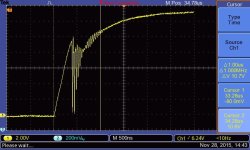
Cap used to load the gate driver is 20nF.
View attachment 3


Zombiess wrote:
One thing I found is that different loads will produce different ringing amplitudes. I've noticed this mainly with the turn on ringing. SjwNz you might want to try a higher inductive load than 9uH. I have 2 load coils I use, one at 5uH and another at 25uH. I like the 25uH because it's closer to the real world inductance I will be powering. I use the 5uH for high current testing since it's dI/dt is faster.
I made a 2nd coil with a much higher inductance just to see if my first coil was causing the issue, but it wasn't, So back to the 9uH and the motor I am using is 12uH.


peters wrote:
So SjwNz, the question is how to reduce the amplitude and frequency of the resonance (as always...). Good laminated power bus has significant intrinsic capacitance, then snubber caps may not be needed, as in Zombiess' circuit, I guess. Otherwise the snubbers should help to solve the problem, but perhaps your cap is not very effective at 22MHz. What is its part number?
Using a WIMA MKP series cap MKP1F033304F00KSSD . I need to get some other values for testing.

You can verify the effectiveness of the snubbers by removing them and doing a pulse test (just carefully, not killing the mosfets). If the frequency and amplitude do not change much then these caps are not applicable here. If they are somewhat higher then the caps have some effect, maybe just not the best type for this circuit.
You need snubbers with the lowest impedance at this new measured frequency, and hopefully not in the inductive region of its impedance (see Lebowski's first link). Also the inductance of the snubber should be much lower than the layout inductance, otherwise it won't have any good effect.
I did this test with and without the snubber caps, and did not make much differences to the gate ring. I have only been using 3 x 0.33uF and don't have any larger values. I ended up soldering 3caps in parallel and then connected them as one cap and did this 3 times for the 3 phases.
This is the scope connected to -BUS and PHASE - Overshot with no snubber - 20Mhz ring - 28V overshot.
No Snubber caps- ring is 20MHz - 28V overshot.jpg

Overshot with snubbers - 23Mhz ring - 24V overshot. wired that ring freq is higher with Snubber caps.
View attachment 1


I did a test today which gave some interesting results.
I increased the distance between the Source and Drain connections between the Hi and Low fets (Phase out) by adding a long length of heavy gauge
wire. So increasing the inductance (I know this is bad) anyway this dropped the ring from 20MHz to 11MHz and the gate ring improved without a G-S cap.
Of cause the down side to this was the OverShoot got up to 86volts (46v battery).
gate with long leads between Hi & Low fet..jpg

For now so that I can use my bike again I think I will decrease the switching times as its very slow with a gate resistor of 40ohms and add G-S caps.
as I know this will help with my ringing issue, but my need to keep an eye on the gate drive with the extra load.
I will have to begin working on a new power stage , to see if I can improve this issue.
I was happy with my first design as it had 1 main laminated bus with fets connect very close to the bus and then very short connections between
the hi and low side fets. O well, if stuff work 1st time I wouldn't be learning much.
 
its interesting that switching a cap is so much nicer than switching a mosfet. like, orders of magnitude nicer. makes me think there is nothing inherently wrong with your gate driver though doesn't mean you won't find the solution there.

i don't have anything on the top of my mind that can help you debug. you could try other mosfet part #. personally your resonance is so bad, if it where me from here it is difficult to solve cause it appears is a resonance problem. , i would probably scrap the design and next time pay more attention to the elements of the system that lead to resonance problem. that reads more harsh than i meant it to be. its just easier to design a product that doesn't have this resonance than it is to debug it on the bench. i been where you are before, i learned the hard way too.
 
Peters, do you have a formula that you use to calculate a proper size snubber cap?
I have some notes on the overshoot voltage, had to search for them.
It is for a simpified circuit with an ideal power supply, one layout L, one snubber C and a MOSFET turning off from high current.
Then the energy from the L plus the energy from the power supply charges the C to a higher voltage until the current is 0. It lasts for a quarter period of the resonance frequency, and the voltage of the C is the highest at this point.
This was the equation:
1/2*L*I^2 + V*I*sqrt(L*C) = 1/2*C*U^2 - 1/2*C*V^2

V is the DC bus voltage
U is the peak DC bus (capacitor) voltage
V*I*sqrt(L*C) is the integral of the power supply current for a quarter period multiplied by the voltage. The supply current after the turn-off is a cosine waveform starting from I and ending at 0, same as the inductor current.

After some calculation the overshoot over the DC bus:
dU = U-V = I*sqrt(L/C)

But it is valid only if the MOSFET turn-off time is about shorter than the time constant of the LC circuit (sqrt(L*C)), and if the snubber C effectively filters the high frequency component (the ~20MHz).
If the turn-off is slower than the time constant then the turn-off ramp limits the overshoot heavily - that is another situation, I don't have calculation for that.
But this formula can be used for sizing the snubber in a perfect circuit (without parasitic inductance other than the main DC bus L...)

-------------------------------------------------

Instead of the phase voltage can you scope the DC bus voltage? I suppose the resonance at the MOSFET drain/source is similar.
But what about the snubber cap pins, is there also this high frequency? This could tell more about the effectiveness of the snubber: if there is no high frequency or its amplitude is much lower, then the snubber is good, maybe just the placement should be changed.
 
well, that's more effort than i ever put in to it. i just used "small, medium or large". small would be 0.1uF, this would be like 1kW drive. 1uF, this would be 10 to 20kW drive. 2uF, this would be like a 50to80kW drive. but then i never started from a position where the initial ringing was really really bad as SjwNz has so i wasn't really trying to fix anything with it.
 
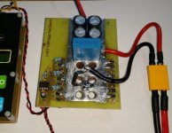
So this is what I have done so I can use my bike again.
Changed my Gate resistor from 40Ω on/10 Ω off to 10Ω on/ 5Ω off, added 20nF G-S cap
Its still not good but is way better than what I started off with. I am still happy with the results for my 1st working
controller, Its almost done 1000kms before I started to do these double pulse test.
G-S cap - no RC snubber across Fets.jpg

Then had a play with adding a RC snubber across the Hi and Low fets and dampened the 20MHz ring and got this
G-S cap - RC snubber across Fets.jpg
I was just having a play and not going to use the RC snubber.

But as you can see in the Gate pic above , only the dip is there no ringing as its been dampened out.
A test I did a couple of post ago, I increased the distance between the HighSide and LowSide fets, which dropped the ring from 20MHz down to 11MHz
and this made a big difference and reduced the ringing on the gate.
Was this improvement caused by me slowing down the dv/dt of the phase outputs ringing so it had less effect on gate via the miller capacitance?
hope that makes sence :)

The 4468 fets I am using have a G-D charge of 80nC, I have found a TO-220 fet with 1/2 this value so will do a 1/2bridge setup with this fet and
see if I get the same issues with gate ringing.


So I connected up my test motor and was running with no load but was nice to see this.


I will try and get a gate shot when the controller is back on the bike with a load.
 
A test I did a couple of post ago, I increased the distance between the HighSide and LowSide fets, which dropped the ring from 20MHz down to 11MHz
and this made a big difference and reduced the ringing on the gate.
Was this improvement caused by me slowing down the dv/dt of the phase outputs ringing so it had less effect on gate via the miller capacitance?
I can't tell exactly what happens, but slower switching should definitely reduce the ringing for sure.
By changing the geometry you probably changed some inductance or capacitance, it could also help.
 
agreed, you changed the resonant frequency and/or your strike frequency. either way, they are farther a part then they used to be to the point where maybe your new snubber with dissipative resistor can effectively mitigate the rest of the "problem".

watch the temperature of that snubber resistor when your inverter is in continuous operation.

The 4468 fets I am using have a G-D charge of 80nC, I have found a TO-220 fet with 1/2 this value so will do a 1/2bridge setup
for the record, although this might work for you, it is not the preferred method. the mosfet needs to be selected with priority for other parameters not the G/D cap. to fix the resonance issue you would change the geometry, strike frequency and/or snubber to dampen.
 
Managed to get a pic of the gate with the controller running under heavy load and even tho the ring is still there, its nice
to see the results you get from a double pulse test translates into the same results when running the motor.
TEK0005.jpg

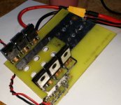
During the week I was playing around with 3 different layout ideas for a 1/2bridge to see if I could reduce the Gate ring.
I ended up getting ringing in all the designs. Lebowski, I even did your low inductance output stage
And still got the ring, but the over shoot was very low:)

Anyway I was getting a bit tired of this dam ring so had a theory about the FETs coss capacitance when peters brought it up earlier.
peters wrote:
The 22MHz can be resonance between the MOSFET Coss and the trace inductance (incl. MOSFET pin). To test it you can add 1nF capacitors between the drain and source of both the high and low MOSFETs, and see if the frequency is lower.

I was thinking if I have more fets in parallel with the inductance of the system it should lower the ring freq which should have less effect on the gate due to miller effect So I quickly made a 3 parallel fet 1/2bridge.
Clipboard02.jpg
Clipboard01.jpg


I did a number of double pulse tests and got up to 300amps (46V battery) and after some playing around with resistor values
and a G-S cap I got this waveform of the gate. The ring freq was 20 to 23MHz in the single fet design and
this 3 fet design droped it down to 13MHz.
(5Ω ON resistor , 20nF G-S cap, and 0.5ohn on each fet)
3fet 300amp DoublePulseTest - Gate turn on(4).jpg

Zombiess wrote:
I've observed that turn on ringing is significantly reduced as I turn on the devices faster. That is I see more turn on ringing on my double pulse testing with a 1000ns switch time than I do at 500ns. I'm not certain on this observation yet as I have not mentally worked through the MOSFET turn on operation and all it's elements
I believe I have came across this as well, I noticed a small drop in the ring size when I dropped the gate resistor value when I was playing with this 3 fet setup.
 
Yes, i know, even with low inductance in the powerlines you will have ringing and overshoot. But the idea of low inductance is to reduce the power dumped in the FET while it is 'zenering', right after you switch it off.....
 
Have you tried a different MOSFET? It could be the MOSFET you have, although reliable, is not suitable for the topology which is in this case a hard switched full bridge. Sounds like this MOSFET might be better suited to a resinance converter
 
Hasn't Zombies had success with this mosfet? I know I used the 4468 and head great luck. I just need to re-design my system with desat for the particular controller that was running them. It was a 18 fet and I think my best was 350 phase amps. Making just over 15hp that's what made the signature picture >>>>>
 
Back
Top