DIY 6FET Controller help

Well, I did some tests with results which probable wont surprise anyone as I pretty much know this was going to happen but still wanted to see.

So at 150amps phase @15KHz PWM the controller would cut out all the time with the smallest amounts of throttle.
I tried to increased Desat to 300amps but I ended up getting 400amps.(I can fix that later)
Controller run good again, but now I knew there was some high current spikes going on which was not good.

I set the Desat current back to 240amps and increased PWM to 30KHz
(Thats as hi as I wanted to go without looking at gate signals, switching times and loads on the gate components. )
It would still trip desat but not as bad and I could ride the bike where as at 15khz it was unride-able.

So now I was a little worried about switching losses and fets getting hot, so I glued a temperature sensor to one of the High side fets (Hiside doing all the PWM switching)
Switch back to 15KHz and rode up a short but steep hill and checked the temp, 57°C.
30KHz and same hill = 75°C

I will stick with 25 to 30KHz and fit a new temp sensor to a fet and the PIC can back off the throttle if fets get to hot, I also need to make a better heatsink
as all I am using is the diecast box which is only 3mm thick and no cooling fins.
Looks like I may have to make a small Dyno so I can do some better tests and get measurements to make sure every is working ok.

So, the controller is now at 150amps Phase and 70amps Avg battery and its just a heat issue stopping me from holding the controller at that level for longer than 1 to 2mins,
which is fine as I am only riding around 1kw most of the time anyway.
I think I may have to increase battery voltage to 50volts soon and then my 2kw controller will be 3kws, happy days.
 
that's a really good result actually. because you knew from theory what to expect. you tested it and found exactly what you expected. and you used that information to determine appropriate operating conditions for your system. perfect.

as a bonus.. you learned something about system design. your motor has low inductance means you have to design differently to get optimal performance. and now you KNOW what that means, at least as far as the gate driver design goes.

ps. let's say worse case sustained operation gave 75C on the mosfet case. i would be OK with that. i don't start to worry until 90C and i have shutdown (or at least a claw back) at 105 (that's even with 175C rated silicon on the datasheet cause the plastic and solder and PCB are not rated for that temp, just the silicon is).
 
Great job!
Controlling these high motor ripple currents is problematic, although the cycle-by-cycle limiting still can work.
At high current - if I understand correctly - the desat circuit was triggered before the current limiter, because the current sensor is slower.
And when the load current is lower than the peak-to-peak ripple then it can fall to 0 in every PWM cycle, then the torque is also 0 in these periods. This problem is similar to a regular DC/DC converter which cannot be controlled (or extra efforts are needed) when the inductor current falls to 0.
As far as I now, for low inductance motors sometimes external inductors are needed in series with the phases in order to increase the inductance. If I remember well, Liveforphysics also mentioned it somewhere. Or the higher PWM frequency is needed.
Do you apply the phase current sensors for cycle-by-cycle limiting?
Could you take some waveforms of your current sensor output with oscilloscope? (current below the ripple current and around the current limit)
 
Hi Peters, my bike is in bits and pieces at the moment as I have been making a new battery box and getting ready to paint the frame.
so will be a little while before I get some scope readings , but yes it will be interesting to look at the phase current and will
have a look at 15KHz and 30KHz. I really need to make a Dyno to do these tests so that mite take a while too.

I was looking at the datasheets for the 4468 fet and the Junction-to-Case was 0.29degC/w. does this mean if the Case temperature was 100°C will the Junction
temp be 129°C.
 
SjwNz said:
I was looking at the datasheets for the 4468 fet and the Junction-to-Case was 0.29degC/w. does this mean if the Case temperature was 100°C will the Junction
temp be 129°C.

From what I understand so far, 129C is the lowest temperature the junction can be if the case is at 100C. The operating Tj is going to be hotter than 129 if the case is at 100C. An insulator such as SilPad 2000 adds another 0.32 C/W if you clamp to 50psi, so now your thermal impedance path is 0.62 C/W. Remember that Tj max is 175 C for most devices. The general rule I've read is a max Tj of 125C for reliable operation and don't exceed 80C on the case.

If you look at the Tjc of larger devices such as SOT227 and larger the Tjc resistance can drop much lower allowing higher sustained continuous current. The problem is the cost goes up, but depending on the application this might be the lower cost option.
 
The thermal resistance must be multiplied by the power dissipated in the FET, and that is the temperature raise of the junction from the case (or from the heatsink or from ambient).
In your case for example if the power loss of the FET is 30W (switching loss plus Rdson loss - these can be calculated), and the case temperature is 100C, then the junction temp is 100C + 0.29C/W * 30W = 108.7C.
But the 0.29C/W in the datasheet is towards the metal side of the FET that face the heatsink, so if you glue the sensor on the plastic side, in that direction the Rth is probably more. For accurate measurement, better to mount the sensor on the heatsink and use the numbers from zombiess (sum of the Rth-s from the junction to heatsink, 0.62C/W or similar).
There are also thermal capacitances that delay the heating up of the case and the heatsink and with the Rth-s they make up an Rth-Cth network, but it is important mainly if someone wants a closed loop control for the junction temperature. - ok I see now you exactly want to do that with the PIC, good luck! :)
 
Calculating the Tj is an iterative process where you have to figure out how much heat is removed and how much is added. I've got some instructions on it it but I have not tried it yet because I don't have any data on how well my heat sink performs.

I have limited real world experience but I have received advice from those who have experience and also from the many white papers I've read.
 
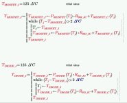
that's right zombiess. start with an assumption that the junction temp is worse case 125C. then, for the steady state condtions, calculate the losses for switching, conduction and quiescent. then for that power dissipation you calculate the new junction temp. the junction temp is also influenced by the heatsink. now you have a new junction temp. so you repeat the process and you end when the difference between successive iterations is <2C. the trick to making this method acccurate is to understand that even for steadystate condition, through the single 60Hz cycle, the current is different pulse to pulse. it's a sinewave afterall on the output, not DC. secondly, the datasheet's curve are CURVED in most cases not straight. and linking the two important facts, its NOT appropriate to linearize the datasheet CURVE because your pulse-by-pulse analysis contains low current (when sine wave crosses zero) and large current (when sinewave is at its peak).

in fact, you can see the interative algorithm in the attached :)
PowerTemp_Iteration.jpg
 
The linearization throws the low/high parts way off on the estimation.

I've been wanting to create an excel spreadsheet to help with this, kinda started on one.
 
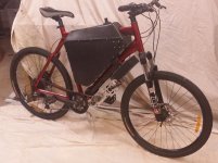
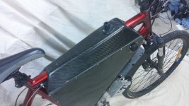
Nothing controller related in this post but finished the new battery box and paint job.
Starting to look a lot better now. still need to clean up the motor/gearbox assemble and Controller case.
Other jobs to do.
-New PCB layout and get boards made by a PCB supplier.( PCBway have been good)
- bigger heatsink and temperature monitoring.
Something I have been looking at for the next step is sinusoidal commutation
after reading a couple of papers and did some flow charts on bits of paper (that I lost)
I will just base it on time between commutations, not sure how well this will work but
will have a play. Not sure if my C compiler will do Sin or I may just make a look-up table.

NBB1.jpg

NBB2.jpg
 
Look-up table should work.
I've been also thinking on a simple implementation of a sinusoidal drive algorithm: the currents must be sinusoidal (not the pwm), so 3 PI control loops for the 3 phases would probably work with a software PLL synchronized to the hall sensors. In a simple case the hall sensor signals can give the time base for synchronization, but better to calibrate them vs. the back-EMF, since they are not perfectly in phase in a real motor. Then the delay of the PI control could be compensated somehow because at high speed the settling time of the control loops can be significant compared to the hall sensor tick (in a hub motor that is about 1ms at 50kph in a 24" wheel).
But the complexity of this can be similar to a sensored FOC, so maybe better to start with an FOC already at first, I don't know. I will experiment with these when I finish my hw.
 
Something that was bugging me from the start when I got this controller working was when it reached max power(Current limit)
the motor would make a strange sound and there was a slight drop in power.
So I would always try and keep the throttle just below the point when current limit would kick in.
I use to think that when you reached max power and open the throttle more the PWM duty would just cut
on every period as cycle by cycle was limiting the power and this would be smooth.
Atfer looking at one of the PWM outputs and loading the motor until current limit kicked in, I could see only some of the pulses had been cut back
at random times so thats the strange sound and then I saw the PWM duty's were disabled for a longer period so that's the drop in power.

So the throttle was directly controlling the PWM duty, but I decided to change my software so that the PWM duty now has a ramp-up and ramp-down delays.
If you open throttle to full, the PWM duty will increase up to max in 500mS or until current limit kicks in.
When current limit is trigger the cycle-by-cycle does its thing and I back off the PWM duty just below the current limit.
So after doing this the controller and motor is now running nice and smooth so I may pretty happy about this.
 
yep, that's called rate control. also you could add checks in your software to make sure there are no instantaneous jumps which must be noise because its impossible for a human to move throttle so fast.

there's a million-and-one of these little things in software and hardware that is needed in the design to make it an actual product (i.e. functional AND reliable). getting the "thing to function" is usually enough for the DIY'er :)
 
I have been a slacker for the last 3months and done nothing on my bike or controller even though I have a number of improvements to do
but with Double pulse testing been discussed in Arlos thread, I wanted to see it I understand this correctly with the Diodes reverse recovery. I really should know about reverse recovery but as I never did any Hipower stuff it never came up. About 10years ago I did made a soild state tesla coil and using a circuit that I based my design on they had a schottky diode in series with the fet and then a Hi speed diode across the Mosfet/schottky. At the time I did not think much about it , but today I looked up the MOSFETs specs and saw its Trr was 560nS to 800nS, so now I realized how slow this is and would cause a lot of heating in the FET as it was running around 300KHz.

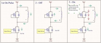
I have a picture of what I see the conventional current flow doing in the Double pulse test and just what to see if I am on the right track.

CurrentFlow on last pulse.jpg
 
Over time reading threads, I have come across the term Snappy reverse recovery, does this mean when current is flowing through the diode in the reverse recovery state,
does the current stop very quickly which I guess is not the best as you end up with spikes, but is good in that there is min switching losses in the diode.
Where as a diode with slow reverse recovery, is better for reducing spikes but shit for switching losses.

Then I have head High hopes talk about silicon carbide which I under stand basically has no reverse recovery.

Or have I got this all wrong and the switching losses is just from the current flowing through the diode and the diodes voltage drop generating heat.
Where the silicon carbide diodes fwd voltage drop is much less so less heat. And the almost zero reverse recovery time is just a bonus so very little if any EMI .

Maybe I should go back to uni :)
 
your first part was correct. and also true that silicon carbide has less losses (due a great deal to no reverse recovery) and also less EMI (since no snappy diode). silicon carbide is a FAST switch though, so you need a gate driver that can keep up and then a way to mitigate the dv/dt noise.

i know it is tempting to focus on acheiving the best possible efficiency.. cause after all doesn't EVERYONE tout their efficiency? 92%, 96%, 98%, 99%! we focus on switching and lesser degree conduction losses like its the be-all bench mark of excellence. but let me tell you, efficiency is only the one aspect of the bench mark.. volume and cost are the others. and these 3 things only become benchmarks after you get a thing to work (functional + reliable). so until you get something to work, don't worry for any of the above 3 things. or in other words.. focus on finding a mosfet/IGbT with nice diode reverse recovery and don't worry about the losses. the thing has to work first! learn all the things you need to learn to design a good working inverter. THEN you will know what you can and can not trade off in your attempt to optimize the 3 goals (maybe efficiency is far more important to you, or maybe cost or maybe a nice balance.. but you can't optimize these things until you know how to make a proper design which takes good guidance and your own product experiment to build your experience)

nice diode reverse recovery goes a long long way to creating a thing that can work. nice diode recovery means a graceful drop with only 3 or 4 humps on the return to zero. recovery is not too fast and not too slow. recovery is somewhat consistent over application range & will grow a lot over temperature (i.e. more lossy) but the ringing doesn't get worse.

all of the above, this is for 10kW or higher. if you're below this power range you have a lot more flexibility. like you could randomly chose a mosfet and it will probably work.. you just don't create a lot a noise at low power levels in comparison to the quality of design which is typical for gate drivers i design (and now ES is starting to design). 10kW or higher, miss the little details and it will crap out on you. its not easy to work at higher power, is why you don't see good examples anywhere nor many "ok" examples.
 
Thanks HH, Lately I have become a bit more interested in the workings of the FETS and the flyback diodes as I have not really looked at that section that much. but yes, I am not to worried about getting better efficiency at this stage as you mentioned I am going for MORE POWER :) well only an extra 500watts. I am so close to that now I am in the process of changing my battery from 12cell to 14cell and that extra 6volts will get me to the 3Kw input power. When I started here 1year ago I just wanted to make something that worked and was hoping for 2Kws.
I still want to do some Double pulse tests and then some scope shots of the bike running at full power.
Once I have done that, I will be re-doing the PCB as it was fine to get me up and running , but was an ass to assemble. then RS232 interface code to adjust controller settings and finally shearing my Code,Sch,PCB if anyone would be bothered looking at it :)
 
Not related to my E-bike but I was looking at a IGBTs short circuit rating of 180Amps for 1mS, Can it handle a much higher Short circuit current for 5uS as with a typical Detsat detect time?
Or will I need to make sure the current will stay under the 180A for any time under the 1mS.
Most IGBTs I have seen have there Short circuit rating based on 1mS.
 
in the datasheet there should be a pulse rating curve. its usually the last one. if it doesn't have the curve, i wouldn't trust the IGBT for use in this application unless it was made by the few "good" manufacturers, then maybe.
 
The IGBT was made by IXYS and I could not find the graph in the datasheets. does not matter to much I was just thinking or adding desat to something I made at work years ago.
Now I am getting interested in making a 2.5kw switch Mode power supply so same power rating as my bike but now working with 300VDC.
Anyway started making a double pulse tester so I can finally do some tests my controller.
 
IXYS makes good product, should be OK to survive a desat protected short-circuit.
 
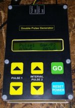
Finally made my self a Double Pulse Generator, Pulse 1 - 3 to 999uS . the interval and Pulse 2 have the same pulse widths and
range from 3 to 100uS with a option to turn off the 2nd pulse. Also added a input for Desat to disable pulses if DaSat is triggered.

DPG.jpg

So I setup the controller with my battery(46V) a 10uH coil connected to +Bus and Phase C. Setup the scope to look at the LowSide FET and Phase C.
Increased Pulse 1 width until I got around 30uS was gave me a current of 150Amps with Interval and Pulse2 set to 5uS.
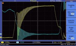
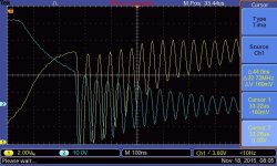
Now this is were I got messed up Ringing on the 2nd pulse on the Gate
Yellow Trace = GATE Blue = Phase

3 - Pulse 2 -15ohm ON, Blue is Phase(Small).jpg

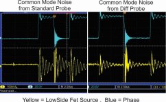
I was thinking it was common mode noise, so did the (Short the probe to its ground clip) and
placed on Source of Low Fet and only got a signal around 200mV which to me did not seem that bad? Then today I was able to
borrow a differential probe and did the same test and the result had less ringing but the same spike so I am mostly happy
all this ringing from the gate is not common mode noise based on the small amount of noise I measured.
CMN.jpg

So I played around adding more Sunbber caps to the bus which did nothing, My turn on time was slow at 3uS with the 40ohm ON resistor, I lowered the Turn on Resistor value to 15ohms and did not make any difference but at lease I got the turn on faster to 1uS.
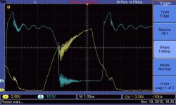
I then added 50nF cap across the G-S, maybe not the best for the gate driver but greatly reduce the ringing.
Yellow Trace = GATE Blue = Phase
7 - 15ohm On 50nF G-S cap, reduced ring (Small).jpg

I started to look at the Phase and Gate and noticed when the Gate was been turned on which causes the Phase voltage to drop to -Bus
when the Phase voltage reached around 12V which is the same voltage as the gate, it started to pull the gate down due to miller effect, which turn the fet off, Phase Voltage would start to rise and gate would recover and FET turns on again doing this over and over until it stabilized. Going over this now is just basic MOSFET miller effect stuff but took me a day to think about what was happening.
Yellow Trace = GATE Blue = Phase
6 - No G-S cap but closeup to show Gate and phase.  (Small).jpg

So it makes me think my gate section has to much inductance due to crap layout or the Gate resistor I am using are rubbish.
 
Are you familiar with these threads (the first one contains about 90% OK stuff, changed my mind about 10%)

https://endless-sphere.com/forums/viewtopic.php?f=30&t=49450

https://endless-sphere.com/forums/viewtopic.php?f=30&t=55641&p=828490#p828490
 
Thanks Lebowski, I did come across these some time ago, but forgot about them.
Had a quick look again today but ran out of time and brain cells.

Before I went to work this morning I looked at the output directly from the 333J Gate driver chip and saw its getting pulled down to 10volts for a short time
Had looked at the Driver chip supply rail and saw 300mV dips on its 15V rail, this maybe to much but its still a long
way from the 333J UnderVoltage lockout voltage of 10.5volts.
To me the drivers output is having trouble keeping its output hi.
I may try a booster stage and see what happens.
 
Back
Top