DIY 6FET Controller help

Njay said:
The inductance between a FET and the exit point to the phase should be tiny; phase current switches between the phase exit point and both FETs, meaning will put those 2 inductances to work (top fet - exit point and bottom fet - exit point). Why not bring both FET rows closer and move the current sensors to the phase board exit points at the board's bottom?
Ok, I see, I also did not like the sensor placement. I made 2 other layout options, but the sensors are at the top edge of the board, because it was better to connect, and the big capacitors are on the left.
Here is Option 2:
View attachment layout_option2_top.PNG
View attachment layout_option2_bottom.PNG
View attachment layout_option2_power.PNG
My problem is the board is larger, 130x87mm, but my target is 130x75 (although not a very strict rule).
The other thing is that the DC link capacitors are 2 different types due to the available area, but probably it is not an issue.

If I push the FET rows even closer in order to fit in 75mm, then it is Option 3:
View attachment layout_option3_top.PNG
View attachment layout_option3_bottom.PNG
The power supply traces are below the lower FET row, this is similar to the draft I posted first a few days ago.
This layout is less symmetric, but the advantage is that it needs only 2 layers, and the drain-source output area (high dI/dt and high dV/dt at the same time) is small as possible. Perhaps it would be good to add a 3rd internal layer anyway, that would be a shielding above the output traces to reduce the stray capacitance (high dV/dt of the output signals), and this shielding should be connected to the GND only at one point close to the power supply input.
And maybe a drawback of this option is that only 2 DC link capacitors fit here, but they can be larger, or can be changed to 3 or 4 through-hole ones.
 
Peters,

Have you calculated the required DC link capacitance and current ripple required for your controller? If not, doing so will allow you to choose the appropriate capacitors. Putting non justified caps for DC link can be a recipe for disaster.

HighHopes posted a great PDF he wrote on calculating the DC link size and requirements with all the needed math formulas. If you can't find it I can post a copy I have later.

What MOSFET, max operating voltage/current and switching freq are you thinking of?

I suspect you might be OK with a 20-30uF cap of the proper type, but the math must be done. Electrolytic a are something you should probably stay away from for DC Link usage.

Do you have a 3rd dimensional size limit?

If you place your current sensors in that location, just remember that you should not have any gate driver traces or circuitry overlapping anything in the power pass. This becomes really important over a 1-3 kW.

Layout is a very difficult challenge. I now prefer external sensors for flexibility in mounting.
 
zombiess wrote
Layout is a very difficult challenge. I now prefer external sensors for flexibility in mounting.

Thats what I have decided to do, I was trying to have them on the power board and have the Gate drivers on a separate pcb with twised pairs
connecting to the fets, but now have decided to put the drivers next to each fet so now I have a single broad design which is look much better now.
I think my PCB design will be ready next week so will post it to see what others think.

Zombiess I think I have HighHopes notes on the DC-Link caps which I found on a different forum but not sure its the same, I will see if I can find it.

I had space on my pcb for 4 Electrolytic caps or two 5uF PP caps that I brought , but was only guessing that the two PP caps was going to be enough.
I need to start calculating and not guessing.
 
zombiess said:
Peters,
Have you calculated the required DC link capacitance and current ripple required for your controller? If not, doing so will allow you to choose the appropriate capacitors. Putting non justified caps for DC link can be a recipe for disaster.
HighHopes posted a great PDF he wrote on calculating the DC link size and requirements with all the needed math formulas. If you can't find it I can post a copy I have later.
What MOSFET, max operating voltage/current and switching freq are you thinking of?
I suspect you might be OK with a 20-30uF cap of the proper type, but the math must be done. Electrolytic a are something you should probably stay away from for DC Link usage.
Do you have a 3rd dimensional size limit?
If you place your current sensors in that location, just remember that you should not have any gate driver traces or circuitry overlapping anything in the power pass. This becomes really important over a 1-3 kW.
Layout is a very difficult challenge. I now prefer external sensors for flexibility in mounting.

MOSFET is planned to be IRFP4468 or 4568, both have advantage and disadvantage.
PWM frequency I use today is 15kHz, but it looks like the dogs hate it, so I want to go higher.

I calculated and made simulations, but my calculations are different from HighHope's pdf.
Ok, let's discuss the theory! :)
I wrote a few points, it is easier to overview:

1.)
I absolutely agree with HighHope's comparison and assessment of electrolytic and polypropylene capacitors, but I don't agree with the calculations in the pdf. My opinion is that this heavily underestimates the ripple current and the needed capacity. Please don't take it personally, we are discussing science.
On page 2 the formula for the cap's ripple current is:
i_ripple = d*(1-d)*Vbat/(f*L)

This is wrong! It assumes there is no DC current on the inductor, and we just switch on the PWM. Then at the end of the first PWM ON cycle, the phase inductor current is iL = d*Vbat/(f*L), but this is not true for quasi steady state, at 50% PWM (worst case) with full DC phase current, so this can't be used for the cap ripple current calculation.

Instead of this formula we have to calculate with the phase current, which is limited by the control circuit, and we switch this phase current on and off from the DC bus. It is true that during the PWM cycle the inductor current also increases and decreases, but that is a secondary effect that complicates the RMS current calculation, so for the first attempt we can calculate with constant (average) phase current. If you doubt it, then imagine a very high L, then the i_ripple tends to 0 by the formula, but obviously it is not true: the bridge switches the phase current on and off the DC bus that makes the cap ripple current.

So the current flowing into the bridge is the phase current, that is the peak current, and the capacitor RMS ripple current is:
i_ripple = i_phase*sqrt(d*(1-d)),
here is an article about this equation:
http://www.eetimes.com/document.asp?doc_id=1273335
Note, that it is the simplified case as I said above, with constant phase current. This is for a single square switching signal on one motor phase. For sinusoidal drive it is somewhat different, because there all 3 phases switch in a single PWM cycle, so the bridge input current waveform has several steps, and the RMS ripple current calculation is more complicated for a full sinusoidal cycle, but the single PWM square signal is the worst case scenario.
So in worst case, when the duty cycle is 50%, the RMS ripple current is the half of the max. phase current:
i_ripple = i_phase*sqrt(0.5*(1-0.5)) = i_phase/2
Then the ripple voltage:
V_ripple = i_ripple/(2*f*C) = i_phase/(4*f*C)

With the example data in the pdf, V=72V, f=20kHz, and let's assume i_phase = 100A at 50% PWM (Pin=3600W), then for V_ripple=4V we need:

C = 312.5uF !!!!

A polypropylene capacitor of this size would easily double or triple the volume and price of a controller. But there are always new products on the market, so I don't reject the idea. If there is an appropriate film capacitor, then it is the best.

2.)
Good/bad news 1:
This calculation is true with an ideal capacitor, as the film caps (nearly), and with a battery with a 'significant' internal resistance, practically 0.1 Ohm, that is usual in a ebike with a few kW power. Without the capacitor the ripple voltage would be 100A*0.1Ohm = 10V.
It is obvious that if the battery internal resistance is very low (many parallel LiPo-s are needed for this), then the ripple voltage and the capacitor ripple current can be lower than the one calculated for worst case. This would need a more complex calculation. The capacitor and the battery resistor together is an RC filter, so when the battery resistance is lower, the ripple current is less square-shaped, and its RMS is also lower. If you design a controller for an unknown battery then you have to design for the worst case.

3.)
Good news 2:
It is also true that in several cases in these controllers at 50% PWM the phase current is less than the half of the maximum phase current due to the battery current limitation. So the i_ripple vs. i_phase curve is different, and when the i_bat max setting is less than half of the i_phase setting, then the capacitor can be somewhat smaller.

4.)
Bad news:
If you use this large polypropylene capacitor, then you have a nearly non-attenuated resonant circuit on the power supply line, practically an LC circuit instead of an RLC, that is switched by the bridge, so you will face heavy high frequency oscillations. From this point of view an electrolytic capacitor is better, but the best would be a large polypropylene with a properly sized serial resistor.

5.)
With electrolytic capacitors the calculation is also more complex, because it is more true that a part of the current is taken from the battery and a part from the capacitor, so the cap ripple current depends on the ESR of the cap and the battery internal resistance. For the ripple current capability, the rule of thumb is 10..20mA/uF, but better to look in the datasheets in every case, and practically the limitation is the ripple current, not the capacity. This is why several 1000uF-s are needed, when el. caps are applied.

Anyway, I'm pretty sure that in most of the controllers, even in the industrial ones, these capacitors are underrated and not designed for the worst case. There are many factors that influence the choice of only this single capacitor, and there are hundreds of other components on a board. The way to do in the industry is that they do highly accelerated life test and stress test with the prototypes that reveal the potential design issues, and from which they conclude the MTBF of the product, and if it meets the requirement (even if it is 5 or 20yrs), then that is considered an appropriate product.
 
For the general case of not worrying about battery <-> controller wiring length/geometry, I always find the PP cap values too small, leading to potential resonance between caps and wiring inductance. Easily seen in simulation, but I know, it's just simulation. As it's just simulation also that I see the snuber caps resonating with the "big" caps, increasing, sometimes by not irrelevant amounts, the RMS current on all the caps. One day I'll measure all this stuff to get to really know.
 
I'm far from a math wiz so I'm going to cheat and use some online calculators for this. Studying this has raised some additional questions for me as well. This mostly me thinking out loud trying to make sure I have my theory correct.

Peters, where is your DC current coming from? With a 3 phase motor the current will be flowing through the inductor in pulses, so wouldn't that make it AC? I can see it going to DC if you reach the saturation point of the inductor because then it is no longer resisting the change in current so treating it as DC makes sense.

If you charge a 50uH inductor with 200A, it is going to take time to reach 200A, it's not instantaneous. If the 50uH inductor has a resistance of 45mOhm then saturation will be at 1600A after 4t=4.44mS. I used http://hyperphysics.phy-astr.gsu.edu/hbase/electric/indtra.html to get these numbers. The 45mOhm number comes from a hub motor I have that's in this range, and 72V as my voltage from the previous example HighHopes used.

50% DC of 20khz is 25uS which puts the current from the voltage source (battery + cap) at 35.6A peak. I can see this peak current needing to be pulled from the DC link but not hundreds of amps (unless the motor inductance is super low or the switching speed has a very long period) before the battery is able to supply the required current.

The main purpose of the DC Link is to supply current to the circuit until the battery/power source is able to catch up and supply current due to the inductance in the power feed, which means twisting the battery feed wires is a good idea to lower their inductance.
I believe the math that HighHopes shared in his write up is the minimum DC link capacitance required, not a hard and fast rule. More than the equation suggests will most likely be required with parallel caps due to the RMS ripple requirements.

The equation you posted from eetimes, i_ripple = i_phase*sqrt(d*(1-d)) only handles duty cycle and current and doesn't integrate voltage, inductance or frequency into it anywhere. It looks like it's only used for calculating ripple current on the capacitor w.r.t. the current output. I see in your math you tried to account for voltage, inductance and switching frequency, but I don't see the relation between phase current and DC link you are trying to show.

In the article they mentioned they did a DFT and took the sum of 10 current harmonics of the electrolytic and a ceramic cap in parallel to get their 2nd graph. Both of those capacitors have different properties and paralleling them turns it into a pretty complex system. I remember learning somewhere (I think a video on EEVBlog) ceramic MLC's don't behave the same an electrolytic and their capacitance changes with their charge level vs an electrolytic, so capacitor construction comes into play as well (they didn't mention in the article what type of ceramic). The first graph does show why 50% duty is chosen, it's the worst case.

Can you elaborate more on why you believe 50% of full phase current should be used for the DC Link calculation? This does not make sense to me as it does not fit within my understanding of the DC link and it's main purpose.

the rule of thumb is 10..20mA/uF, but better to look in the datasheets in every case
I've never heard this before and it doesn't make much sense. What type of capacitor, there are lots of types with different properties, what ESR, what frequency, what charge level, etc? Datasheets make a lot more sense.

This question is for HighHopes for the i_ripple = d*(1-d)*Vbat/(f*L) formula and the C=Vbat/(32*L*C*f^2)

Where does the 32 come from?

How does the resistive component of the L effect the ripple current demand. If the 50uH inductor is 1mOhm vs. 45 mOhm, wouldn't the require capacitance increase as the inductor resistance went down due to the increase of di/dt or was the R component zero'd out and removed from the equation for a worst case scenario with the indutors resistance being zero?

I've been using lots of formulas I find in papers for electronics for many years, but now I'm trying to understand why they work so I'm attempting to learn the math (calc/trig/algebra). It's tricky but awesome. Eulers formula and the Fourier transform are amazing!
 
The phase current should not change too much in a PWM cycle. If it changes too much, then it easily goes down to 0 or up to the upper limit in a few PWM cycles, then the current is not controllable properly with a closed loop control, because the current control loop works at the PWM frequency, or even slower. "Too much" current change is a design trade-off question of PWM frequency, motor inductance and supply voltage. If the motor has too low inductance and the voltage is high, then the frequency must be increased. The worst case from this point of view is the start of the curve in the current vs. time diagram on the link you sent. For a 50uH motor the 20kHz is a too low frequency, because starting from i=0 after one 100% PWM cycle the current is 70.4A, that is too much change to control.

The maximum allowed phase current is another thing, it is not linked to the inductor parameters, because it is controlled by the control loop with varying the PWM duty cycle. When the high side FET is ON, then the phase current increases a little bit, and when it is off, then it decreases also a little bit. When the high side FET is ON, then this phase current is pulled from the power supply, so this is the DC bus current from the capacitor and the battery together.

zombiess said:
The main purpose of the DC Link is to supply current to the circuit until the battery/power source is able to catch up and supply current due to the inductance in the power feed, which means twisting the battery feed wires is a good idea to lower their inductance.
No, it can be acceptable only if the power supply has a very low output impedance, for example the big capacitors are placed at the output of the power supply. But it is not our case, because the battery has the ~0.1 Ohm resistance (more or less). So in our case the purpose of the DC link capacitor is to filter the DC bus current from the PWM frequency and to keep the ripple voltage low.

In the deduction of the equation at eetimes they subtracted the DC component from the bridge current, and the result is the AC capacitor current. It makes sense, because the capacitor has no DC current, only AC. Practically it means that the sum of the the battery current and the capacitor current is the bridge current, and that is a rectangular current due to the high side FET on-off switching. They calculated with RMS values, this is why they used the square of the RMS currents. An RMS AC and a DC voltage or current can be summarized this way. The maximum of the capacitor RMS current is at the 50% PWM as seen on the curve, and this RMS current is the half of the phase current (from the formula), because the phase current is the peak current to the bridge in our case.

The formula of V_ripple comes from the equation of the capacitor: i*dt = C*dV. This is very simple: if we connect a constant i current to a C for dt time, then its voltage is raised by dV. In our case as the ripple current is approximated with a constant for a half PWM period, the V_ripple = i_ripple*dt/C, and dt is the half of the PWM, so dt = 1/(2*f), then V_ripple = i_ripple/(2*f*C) = iphase/(4*f*C).

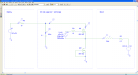
I made a pspice model, that explains the situation better, because calculations become very complex after just a few components.
Here is the simplified schematic:
01 schematic.PNG
The low side FET is there for its body diode, because when the PWM=0, the inductor current goes through it.
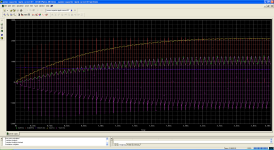
When we start the PWM, these are the graphs for the first 3 ms of the transient simulation:
02 all signals 3ms.PNG
The yellow curve is the phase current, in real systems when the control loop is in operation, the current would ripple around 100A (or whatever the phase current limit is). In this simulation there is no closed loop control, so it slowly increases step-by-step with the PWM frequency, and saturates after a few ms, but it does not effect what we are interested in.
Let's assume the real life control loop keeps the current around 100A, so I zoomed into the 100A area for a PWM cycle between 500 and 550 us.
03 phase current.PNG
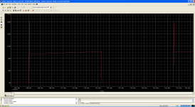
The red curve is the input current to the bridge (high side FET), it switches between 0 and the inductor current. The glitch at the rising edge is only the reverse recovery current of the low side FET body diode (not sure if it is accurate in the pspice model of the FET).
04 high side FET current.PNG
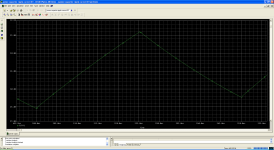
The green curve is the battery current. If the DC link capacitor was missing or would be too low, then the battery current would be the same as the bridge current, swinging between 0 and 100A.
05 battery current.PNG
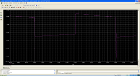
The purple is the capacitor current, it ripples from -50A to 50A, not exactly square, but nearly. 50A is the half of the 100A phase current, as calculated, and this current goes in and out of the capacitor. Its RMS is the RMS ripple current, that is 50A. The inductor parameters (L and R) and the practical battery resistance effect only the slope of the high and low levels (the slow increase and decrease at the top and bottom), but the approximate 50A and -50A is always there.
06 capacitor current.PNG
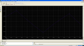
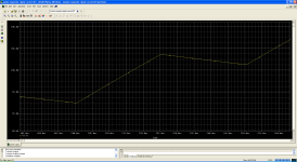
The blue curve is the DC bus voltage, in this circuit the ripple is about 2V. By calculation it is the same: V_ripple = 100A/(4*20kHz*625uF) = 2V.
07 DC bus ripple voltage.PNG
You can put this schematic into pspice and change the values or add a serial ESR to the capacitor or DC bus inductors and see what happens. Simulations adds a lot in understanding how the circuits work.
 
I found HighHopes PDF for DC-Link caps.
viewtopic.php?f=30&t=31804&start=50#p839118

FYI, that post was not meant to be a definitive guide to calculating an optomized uF value of DC link cap. we were discussing the merits of electrolytic cap vs. poly cap and my position was that poly is way better (type MKP). the post was meant to show how a poly cap is NOT more expensive than an electrolytic capacitor in this application and will take up less volume and perform better. i used some math to make my point. mind you, if you had no other way to estimate what uF cap you want, the document will get you in the ball-park, but its not meant to be super accurate.
 
ehhhh... how about adding at least bat wire inductance and the already mentioned cap ESR, plus cap ESL?
 
The glitch at the rising edge is only the reverse recovery current of the low side FET body diode (not sure if it is accurate in the pspice model of the FET).

that's probably accurate. reverse recovery is aggressive, high spike of current in fast frequency. its probably the second most important factor in what defines a good mosfet for this application or not. (first most important is ruggedness).

ps. silicon carbide mosfets do not exhibit any reverse recovery behaviour :)
 
Peters, thanks for posting the simulation. Do you mind sharing the PSpice file?
I think I see what you are trying to show in your example.

I have some questions which may or may not be applicable.
What happens when the load becomes very dynamic such as spinning motor where you have an inductor moving in a magnetic field generating BEMF?
What about multiple magnet poles and stator teeth?
Different operating conditions the motor experiences such as sudden acceleration (like wheel slip), regen, sudden stopping such as locking the rotor like a panic stop.
Operating load conditions?
Does being 3 phase vs single phase AC on the output change how it behaves?
 
HighHopes said:
FYI, that post was not meant to be a definitive guide to calculating an optomized uF value of DC link cap. we were discussing the merits of electrolytic cap vs. poly cap and my position was that poly is way better (type MKP). the post was meant to show how a poly cap is NOT more expensive than an electrolytic capacitor in this application and will take up less volume and perform better. i used some math to make my point. mind you, if you had no other way to estimate what uF cap you want, the document will get you in the ball-park, but its not meant to be super accurate.
Ok, but our calculations are fundamentally different, and the result for the needed capacitance can differ by 10 times multiplier...

Njay said:
ehhhh... how about adding at least bat wire inductance and the already mentioned cap ESR, plus cap ESL?
Then we add some high frequency oscillations. As you said above, the simulation with inductances can be different from real measurements, and I think it is because the real supply lines are distributed parameter transmission lines, especially when the power bus planes are laminated to each other. That is not only a reduced inductor, but has an increased distributed capacitance. This could be modeled with a lot of small LC circuits.
Adding ESR modifies the current division between the capacitor and the battery.

HighHopes said:
ps. silicon carbide mosfets do not exhibit any reverse recovery behaviour :)
Ok, It's good to know :)

zombiess said:
Peters, thanks for posting the simulation. Do you mind sharing the PSpice file?
I think I see what you are trying to show in your example.
No problem, I attached the file. It is made for PSpice v9.1 student edition, it is not a new version, but I think still widely used.

What happens when the load becomes very dynamic such as spinning motor where you have an inductor moving in a magnetic field generating BEMF?
BEMF is simulated by the voltage source in the motor model. Now it is set to 0, but can be any other. When the voltage is higher than duty_cycle*72V, then there is no effective motor current. That would be regenerative braking for which the low side FET should be switched, too.

What about multiple magnet poles and stator teeth?
I don't exacty know its effect. If they introduce some torque and current ripple, and its frequency is lower than PWM then it would be compensated by the current control loop.

Different operating conditions the motor experiences such as sudden acceleration (like wheel slip), regen, sudden stopping such as locking the rotor like a panic stop.
Operating load conditions?
I suppose the mechanical transients are usually slower than PWM, so the control loop should limit the max. current. If there is a very fast transient, then the current may increase for a while. Or if the current control loop is slow, then there would be a current overshoot for some time, but that is not a good design.

Does being 3 phase vs single phase AC on the output change how it behaves?
Yes, definitely. I calculated only the most simple case. For 3 phase I did not dig into the details, but for simple trapezoidal drive it must be the same, because one phase is switched at a time in every 6 commutation states. This is for unipolar PWM. At bipolar PWM the overall switching frequency on the bridge input is the double of the PWM, so the needed capacitor is maybe the half of the calculated, this could be checked by simulation, but I've read somewhere it adds harmonics to the motor current and reduces efficiency. In 4-quadrant drives it is probably more complex, because there is reverse current from the motor to the capacitor in every PWM cycle.
For sinusoidal drive, it is even more complex to consider, because the duty cycle change in every PWM period with the sinusoidal waveform on all 3 phases. The bride input current is not a (nearly) square wave, but a sum of several square waves with different duty cycles. Finding the worst case in terms of capacitor RMS ripple current would be interesting.
 

Attachments

  • power capacitor ripple current 03.sch
    5.7 KB · Views: 37
I was thinking more on the sinusoidal case, and now I find possible that HighHopes's formula is the correct one for the fully symmetrical sinusoidal drive, and mine is not applicable in this case.

Because maybe there is no large current transfer between the capacitor and a motor phase in any state of the PWM, and the ripple current of the capacitor comes from the inductor ripple current only. If it is true, then the current from the power supply to the bridge is nearly DC throughout every PWM cycle, independently of the peak-to-peak sinusoidal voltage. I will need to check the sinusoidal PWM method and the currents to confirm this.
 
I was thinking more on the sinusoidal case, and now I find possible that HighHopes's formula is the correct one for the fully symmetrical sinusoidal drive, and mine is not applicable in this case

lol no worries. we're just discussing theory. in my experience, i just use 10uF per kW and size the cap that way. ha! only volume driven applications really benefit from any sort of time spent calculating an optomized uF cap. there are many factors that go into sizing the capacitor but what i found, when i did this math in high level detail with PSpice simulation as well, was that usually one factor dominates the sizing and usually that scenario appears when motor at rest and suddenly full torque is applied.

i know that everyone cares for volume, so shouldn't we make a deep analysis to get exact uF? sure if you have time.. but, what i mean by volume driven, is if saving 1 cubic centemeter gives you value of >$1000 then you have a volume driven application and you should definately make the analysis. if such savings is worth practically nothing to you because your car/ebike/emotorcyle has at least 1 cubic cm to spare.. then don't waist your time; follow my doc (or your own method) and that's good enough.

i think when these projects (Swyz, arlo, zombies, my own) are all said and done we need to collect all these thoughts into a cohesive "this is what works AND WHY" document for future practitioners.
 
HighHopes said:
btw peters, you might be interested in my post #2 over here http://ivanbennett.com/forum/index.php?topic=112.0

Nice thread over on that forum on your development.

I want a hardware platform to develop and test software on that I can run a hubmotor. I've been looking at IXFN360N10T SOT227 modules which aren't cheap (at $19 ea in 10 qty) but would seemingly simplify a prototype platform for software development and testing at more than token power. 72V is just right for my CroBorg, and whatever current is practical from these "200A max" devices should be adequate for what I'm interested in doing, and reasonable power for my CroMotor. The infineon chips are unobtanium, so I'll probably go with a different one, perhaps the ACPL-333J that has been discussed. Just studying the various threads at the moment, will make a separate thread when I get ready. Great to see a design example with these modules, haven't seen much on them here at ES.

Thanks for everyone's contributions to these threads!
 
Alan B said:
The infineon chips are unobtanium, so I'll probably go with a different one, perhaps the ACPL-333J that has been discussed.

I have a sorted out TD350E driver setup. It can be made usable up to about 30khz with a minor tweak, but usually 10-20khz is all that's needed for a motor drive. Will save you a ton of time designing a gate driver from scratch. It's much harder than I ever imagined it was going to be, app notes and spec sheets just don't give enough information, many gotchyas and a giant do/don't list. There is a big void in gate driver / power electronics learning material. I most likely would have failed miserably if I tried to do it without the help I received.
 
Have been working on a layout and was thinking about the best way to connect the GNDs of the input side of the HiSide Gate drivers.
This layout is not complete so it is missing connections so hope I am not wasting any ones time, but I just did this layout
to mostly show the GND connections. As you can see from the PDF there is a large gnd ring which I am worried about
as I think this forms a loop?

I was thinking about just using ribbon cables to the Hiside drivers and remove that ground ring, but will see it this attached PDF
gets the thumbs up or down.

View attachment GND Track layout Ideas 1b.pdf
 
looks ilke you are using DC link negative terminal as connected also to your digital ground. if you do that, there is no need for half the ACP-333J you have on the board and also you will be limited in the power range (dunno if you will get the 150A you want).

once you fix that problem, the ground loop issue will go away.

also, are your mosfets goingto share a common heatsink? they should.

also, you might consider making the void around DC link cap terminals a bit bigger. bad for canceling magnetic fields, but in this case the reduce chance of flash over due to cap leg soldering blob would probably be worth it.
 
zombiess, would you mind posting that ground layout plan, generalized grounding plan, we refined via PM?
 
HighHopes said:
zombiess, would you mind posting that ground layout plan, generalized grounding plan, we refined via PM?

This one? I need to add the key and then it's done unless you have any other comments to add to it to make it more clear.

gate-driver-ground-planes-draft.jpg
 
Back
Top