Vasili said OK...so here goes...
NOTE: The word "teardown" does not imply ripping apart the controller and saying it is garbage. It just means "taking something apart to see all the inner workings".
We've all seen this image previously. The board in my 24 fet controllers looks pretty close to the same. If anything the orientation of the mosfets and 3 more large electrolytic caps is all I can tell is different from this picture.
This is essentially the same size of two standard 12 fet controllers crammed together onto the same board. The effort put into making what may be the smallest 24 fet and still use TO-220 mosfets is pretty impressive! For people like me that can repair electronics, this is still serviceable and yet very compact.
This is a heat spreader like I'd expect to find in any 12 fet controller but there's 2 of them in the 24 fet Nucular.
This is a PV sinusoidal 12 fet. Basically...Vasili used nearly the same board space better. He put all the control electronics and DC-DC on daughter boards and put another row of mosfets down the open edge of the board. This makes a Nucular 24 fet controller fit in nearly the same amount of real estate as a typical 12 fet controller.
A few close-ups of the board. Everything is coated in conformal. This cap is pretty much the biggest thing you can fit in the space! Notice the ceramic insulators behind the mosfets.
The MCU daughter board is very similar to the one in the 12 fet (second image). A modular design makes design costs lower. All you need is slightly different firmware and possibly more mosfet drivers and the same daughter board works in the 12 fet or 24 fet.
The DC-DC board (first image) looks like the one in the 12 fet (second image)too.
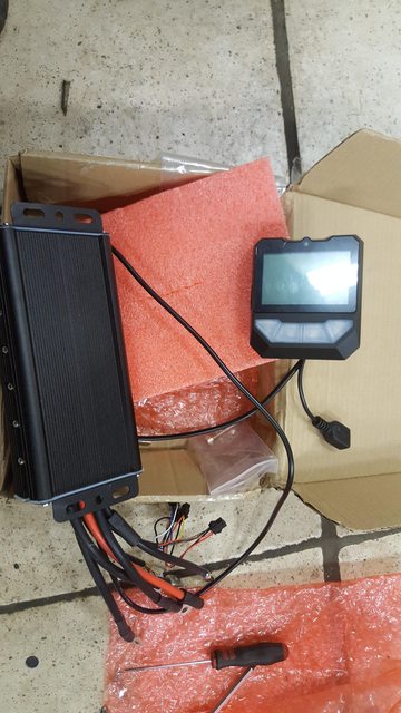
You still have this internal bank of connectors.
In the right center is the BATT- power buss with 4, 1 watt .001 Ohm shunts. There's no visible copper here which seems odd. Maybe there is a beefy copper layer inside the board for the BATT- power plane? The reason why you see an "oval" at BATT- is so that the large filter caps which are placed on both sides of the daughter board can connect to BATT-.
In these images you can see "something" on the top side of the board at BATT-. It's hard to see down there, but I think there might be 4 more shunts here and maybe copper?
In this image you can see how the 3 phases are laid out. AKA...3 sets of 8 mosfets. 2 phases are on either long edge of the board and the third phase is oriented around the remaining space at the end of the board. My original guess, and this is becasue I've seen it done several times, was the 3 phases would be in 3 sets across the width of the board. See the second image from a Sabvoton controller. I'm sure a layout like this was tried and maybe it was too difficult to route power busses and other things around them? The phases all have added copper on the bottom of the board.
Close-up of the third phase that wraps around the end of the board.
The other 2 phases. Nice copper reinforcing. Something I like about Nucular controllers is the attention to detail. Notice the "fingers" coming off the main copper buss that go right up to the mosfet legs. This minimizes the amount of solder needed to connect the mosfet leg to the power buss for the phase. The center solder connection on the left edge is BATT+. There has to be an internal copper buss inside the board for this.
This is 2 phase wires and the red BATT+ wire coming into the top of the board. Notice how the BATT+ wire has no large trace coming off of it. I'm really curious to know how thick that inner copper trace is! According to the specs on page 1 it is capable of handling 300 amps.
It's hard to see in the image, but under the screw for this mosfet is a tiny board with a thermistor on it with 2 grey wires coming off it. There's not one on the other row of mosfets that I noticed.
The shell is somewhat thin IMHO. Maybe this isn't an issue? I don't really know yet. This controller is sooo small and I have zero experience running it. I'm really curious about how well it performs and how well it stays cool. I have an 18 fet PV controller that I run at 200 phase amps, 82v and 100 battery amps. It is about the same size as the Nucular 24 fet, but has a lot more surface area in the shell. I have a fan blowing on it so it stays cool. I'll be putting one of these controllers in place of that PV 18 fet soon.
This is a current PV 12 fet controller shell. I looked for an end view image of an 18 fet PV shell and don't have one, but it is like this too. The aluminum walls are about 1/3 thicker than the Nucular shell with a lot more fins.
Fitment inside the shell is really close! I wonder how you could make this a tighter or closer fit. I'm tempted to add a piece of epoxy-glass sheet under the board like I do for all the PV controllers I mod.


I did find one thing that is a bit worrisome. Notice how some of the legs of these mosfets don't have good solder flow. You shouldn't see empty through holes on a mosfet leg. The solder ought to flow up the mosfet leg and onto the wider section of all 3 legs. I believe the mosfets are hand soldered in place. Looking at the bottom of the board at the mosfet legs, looks like decent quality hand solder work to me. Anyway, solder didn't consistently flow up through the holes fully and onto the wide section of the mosfet legs. I dip my mosfet legs in flux or pretin them before soldering them in place to eliminate this issue. The center leg is Drain and the right leg is Source. This is the current path through the mosfet. The left leg is the Gate and it doesn't matter too much if it is lightly soldered or not. The thick section of the mosfet leg is rated for 75 amps while the lower section about half that. The mosfet legs will heat up as a result and add heat to these mosfets.

") Pretty please!
Pretty please!