ZombieSS's power stage for Lebowski's controller video pg17

I decided for initial testing I wanted to use a latching shut down

i think that's good for development testing.. but i wonder for normal operation. while driving on the road.. do you want to shut down all of a sudden? maybe a chirp-restart is in order? autmoatically restart the drive after a fault (shoot-through for example) just make sure you leave enough time to cool off the mosfet before restart.. maybe 0.5 second is long enough. if 3 faults in a row then must mean the fault is persisting so THEN you might as well shut down with latch.
 
this comment comes from arlo's thread but i didn't want to continue discussion of your design over there..

on the subject of parallel mosfets and pull-down resistor & G/S caps.

I put one at each location due to symmetry. I'll gladly drop to a single G-S cap/resistor if you think it's ok. I could place it right after the gate resistor.

if you have ONE G/S cap or one per mosfet, it is NOT symmetric to put one cap per mosfet. think of it as putting 5nF per mosfet. if you measured each cap, maybe the first one is 4.98nF, the second is 5.5nF, the third is 5.0nF.. etc. is it still symmetric? no.

but if you have just ONE G/S cap, 30nF,es.. and you measure it to find in reality it is actually 31nF, is the design still symmetric? Yes.

remember, it is from the view point of current sharing in parallel mosfet that we make this discussion. the more the design encourages symmetry, the better.
 
HighHopes said:
this comment comes from arlo's thread but i didn't want to continue discussion of your design over there..

on the subject of parallel mosfets and pull-down resistor & G/S caps.

I put one at each location due to symmetry. I'll gladly drop to a single G-S cap/resistor if you think it's ok. I could place it right after the gate resistor.

if you have ONE G/S cap or one per mosfet, it is NOT symmetric to put one cap per mosfet. think of it as putting 5nF per mosfet. if you measured each cap, maybe the first one is 4.98nF, the second is 5.5nF, the third is 5.0nF.. etc. is it still symmetric? no.

but if you have just ONE G/S cap, 30nF,es.. and you measure it to find in reality it is actually 31nF, is the design still symmetric? Yes.

remember, it is from the view point of current sharing in parallel mosfet that we make this discussion. the more the design encourages symmetry, the better.

So your suggestion is to drop the individual parallel G-S caps/resistors and just use one of each after the gate resistor. I like this. The current setup I am using right now has 1 4.7kohm G-S resistor and then 4 15nF G-S caps totaling 60nF (they are in parallel) per high / low side. In my new design I just posted last night, I will correct this. I twill make the layout much cleaner too.
 
Jasmine said:
:D Dear Zombiess, you must be a considerate person who is professional, I like your talking!

Not sure if genuine or spam bot. If genuine... thank you. I see you have Pintech listed as your website, I'd like some of their differential / current probes for my scope :)

I wonder if you got here by searching for "differential probe" ? :D
 
i think jasmine got here by searching "champions of the world" .. just my guess is all
 
Did a bunch of bench testing today to get my G-S transition time to around the 1uS mark. It was around 3.2uS 0-10v with 60nF G-S cap and a 20 ohm gate resistor.

I have been exchanging PM's with HIghHopes about the G-S transition time. Here is a snippet he sent me about tuning the G-S transition time because I noticed mine seemed slow and some of my G-S pulses on the same phase/side were running together a little bit and that didn't seem like a good thing.

i have learned that measuring D/S voltage is not that useful other than to get a sense of how fast the switching is. i don't even look at how much ringing there is because the frequency is so high i can not trust that it is real (i.e. would it dissapear if i removed the probes?).

keep the gate resistor within the range acceptable to the mosfet datasheet
start with the highest resistor, maybe 20 ohms (but read you're datasheet) if heating of mosfet is acceptable at highest gate resistor then you're done. we don't worry about D/S switching speeds because gate resistor is WITHIN datasheet parameters so your worse case deadtime calcs are still valid. D/S switching speeds then are as slow as it can be for this mosfet and we pray it is slow enough to not suffer from noise problems. but its a good prayer because we build the inverter with quality parts, laminated bus-bar, structured approach to gate driver design & layout so we know our system can handle some noise without difficulty.
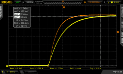
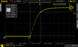
So I looked through the IRFB4115 datasheet and was unable to find any graphs relating to gate resistors and can't ever recall seeing them on a MOSFET datasheet, but I've only looked at a few. I have seen this parameter on IGBTs, not sure if it's specific to them.

I decided to try some experiments to drop my G-S transition times and see how things turned out. With the setup as it was, 60nF G-S caps and 20 ohm on/off resistors it my G-S transition of 0-13V was taking 7.5uS... kinda long. D-S was happening in about 300nS.

First test was reduce the gate resistor down to 10 ohms on / off and remove all but 15nF of the 60nF of the G-S caps.

Here is the difference with a 10 ohm gate resistor and only changing the G-S capacitance
turn on
g_s_15nf_vs_60nf_10on_4r7off.png

turn off
View attachment 6

I eventually decided to keep the 60nF worth of G-S caps on each 4 paralleled MOSFETs because I noticed I was having some odd false triggers from my error detection circuit which would shut down the PWM. I wasn't able to track it down the cause, but the difference from 15nF to 60nF was the difference between a working fault detection circuit vs false triggering. It worked ok at 30nF of G-S cap with a 30V buss, but when I went to 60V it was false triggering occasionally again. I verified it wasn't anything with switching speed by swapping back the 20 ohm gate resistors, still had false triggering problems even though the G-S on time was now much slower.

I am working with isolated supplies powered by the mains and I get some noise on the traces with regular probes, some really goofy looking waves with peaks that would kill the gate that made me suspect the probe was causing an issue. I switched to my 30yr old differential probe and got a totally different picture. Night and day difference, WOW!

So here are some of the scope shots I managed to get when I finally decided on my G-S cap and on/off resistors.
On resistor = 4.7 Ohms
Off resistor = 1 ohms
G-S capacitance total per bank of 4 MOSFETs = 60nF

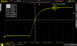
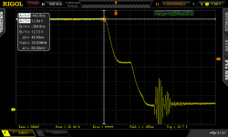
The result was a G-S 0-10V on time of 1uS. I did notice I was still picking up some odd noise at times and it appears to repeat in a pattern. I believe what is seen here is caused by the other banks firing off. I selected the worst examples that I captured to post here. The ringing has a frequency of 20-22Mhz and it shows up at different levels no matter what probe I use. The differential provides the best results which is what I used for the below screen shots.

Here are 3 screen shots showing the 22mhz ringing appearing at 3 different locations in the on transition.
View attachment 5

g_s_1us_on_ring2.png

g_s_1us_on_ring3.png

This is a shot of the turn off, the ringing appears at different spots, but here it's right after the miller clamp
g_s_2us_off_ring.png

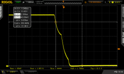
What most of the recorded wave forms look like.
g_s_1off_2us.png

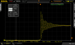
I also did some D-S shots, but not with the differential. I only saved one to show the extreme ringing that I was seeing. It's the same familiar 20-22mhz frequency
d_s_ring.png

To summarize, my controller now has a 0-10V G-S transition of ~1.0uS, 2.5uS to get to 13v which is the max
My G-S off time is ~2.0uS

I measured the D-S on/off time and they were ~175nS on 125nS off, both have some +20mhz ring in them for about 1uS, nothing as bad as what is seen in the above example made with the passive probe.

My G-S pulses never run together now, there is always a ~800nS time between the closest pulses but the previous pulse goes full off before the next one goes full on so I believe I am OK now.

An interesting side effect from speeding up the G-S transition is my dead time changed by a large amount when I retested it. I had been at 650nS with the 20ohm gate resistors and 60nF G-S caps. On the new setup I have tested as low as 50nS dead time and my current didn't spike up at all, nothing got warm, but I did notice when reviewing wave forms that I had some of the G-S pulses not fully turning off before the next one turned on. Setting the dead time to 500nS gave me ~800nS as the shortest. With the 20 ohm gate resistors the best I could ever get was 450nS for my dead time before running into shoot through around 400nS. Anything below 400nS = high current draw and warm heat sinks.

I tried experimenting a little with the switching frequency since dead time is low. I went to 24khz and everything looked good on the bench test / scope.

Anyone have an idea as to what my 20-22mhz noise is in a lot of the shots? Should I concern myself with it or just move on. Trying to make measurements in a noisy environment is very hard because it's difficult to tell what is real. An FYI, I scoped the brain board and also noticed this 20-22mhz noise happening on the fault signal pin. I suspect it's the scope or the probe picking it up and it has something to do with the motor. When the motor is in sensored mode the noise is stronger and then in sensorless mode it drops to a fraction of what it was.

I tested the high side drain to low side source to get an idea of what was real, I only picked up a 1v p-p blip and it wasn't anywhere near 20mhz.
 
I noticed I was having some odd false triggers from my error detection circuit which would shut down the PWM
that's really important. teh gate resistor (and maybe G/S cap if you need it) are there to find the balance between mosfet heating and noise generated. so when you have error detection giving false trigger when D/S switching is fast and no error when D/S switching is slow, this is a good sign that you have found where your limit is. in my experience switching DC bus voltage in < 200ns means you will have a lot of noise likely more than what a standard gate drive design can manage. and from what i know of MOSFETS they are designed to switch fast which is not exacty the same as IGBT. so perhaps your instincts of switching speeds and how to achieve them (gate resistor + gate cap) so avoid noise problems is good.. seems the right path to me. make sure you can manage the heat rise, and you're done.

some other comments:

you should not be changing your deadtime. the deadtime is a worse case value chosen analytically (see my post on this i think in arlo's thread). if you speed up the D/S switching because your lower gate resistor then you simply have more margin in shoot-through prevention. if you lower your deadtime because you are switching faster, i would say only do this if you have a need (i.e. your deadtime represents >5% of your switching perioid) and be careful you understand HOW to do this, i.e. how to know exactly how much you can lower it by.

i checked your mosfet datasheet and another one at random to see if i could find the graph that shows Rg vs. Rise/Fall timing.. but it is not there. perhaps you are right, it is a common IGBT graph but not MOSFET? only clue on datasheet for IRFB4115 is shown in dynamic portion, right hand side they used an external 2.2 Ohm resistor to get all their numbers. generally a gate resistor in a real life circuit can never use so low a value that the manufacturer chooses in thier dynamic section of datasheet. i would say in a range some where between 2x and 10x that value, so for IRFB4115 try to stay greater than 4.4 Ohm and less than 22 Ohm to stay within the expectations of the manufacturer.

as a side note, i did notice your mosfet has an internal gate resistor value of 2.7Ohm which may imply you do not need the external 0.5 Ohm and also makes me wonder if your spreadsheet math for calculating gate drive parameters & sizing takes this into consideration? if you put external 10 ohm for example, the internal represents almost 30% addition.. could make a noticable difference in your math.
 
HighHopes said:
as a side note, i did notice your mosfet has an internal gate resistor value of 2.7Ohm which may imply you do not need the external 0.5 Ohm and also makes me wonder if your spreadsheet math for calculating gate drive parameters & sizing takes this into consideration? if you put external 10 ohm for example, the internal represents almost 30% addition.. could make a noticable difference in your math.


I too noticed this yesterday an added it to my spreadsheet. If I would have been paying attention before I probably could have asked about the 0.5ohm resistors being needed, so I'm glad you brought it up. I'm thinking we do not need them for MOSFETs that have an internal, but adding them doesn't really hurt since they are only 0.5 ohm and a 0.0 ohm could be installed as a jumper, cheap nice to have option. I was also thinking that having the ability to adjust this value is good to have in addition to the gate. Between the gate resistor, g-s cap and g-s resistor the happy medium should be able to be found.

Thanks for your input on the noise I noticed. Without my really sensitive fault detection PIC Micro monitoring things I wouldn't have found out what was going on until things got really bad, the controller continued to work just fine after I installed the bypass jumper without any errors. They way I approached this error was by removing all but 1 of the G-S caps on the high side of phase B and things usually worked OK, but would sometimes fault. This made me curious so I added a 2nd G-S 15nF back and the faults stopped. Tried multiple times to reproduce. Went to phase B low side and removed all but 1 G-S cap, problem came back and it still had 20ohm gate resistors so I knew the G-S caps were somehow involved. I kept playing with on/off resistor values, but none higher than 20on/20off and figured out the false trigger was G-S cap related. With 60nF G-S cap I was able to run 1ohm resistors in both on/off and not trigger faults, but had gate ringing at turn on. That's why I settled at 4.7 ohms on and 1 ohm off.

If this holds up under higher current use then I should be OK, only further testing will tell and that requires high current battery power and a bicycle.
 
Lebowski said:
The 20-22 MHz looks like the typical ringing of the mosfets output cap with the power line inductance. Place 10nf across each cet and you'll see the frequency change...

What is a cet?
 
Njay said:
it's a typo... fet.

And where exactly should this cap go? I would like to experiment with this just to verify. Already learned a ton more about tuning on the bench yesterday. All the math I've seen for picking a gate resistor are worth about zip. Needs to be done on the bench with a scope. Dealing with the noise issue and my fault detection circuit was VERY educational, not sure how close I am to the limit with 60nF, but 15nF was not enough and the issue didn't change with higher value gate resistors, only adding back the G-S caps solved it which seems to be a bit of an unorthodox solution, but one that works with what looks like very little down side (a designer might need a larger wattage gate power supply)
 
Drain to source. Leb is saying to artificially increasing the "fet output capacitance" to test the hypothesis that the ringing comes from it, by seeing a change in the ringing frequency (which should be lower with the 10nF cap).
 
Njay said:
Drain to source. Leb is saying to artificially increasing the "fet output capacitance" to test the hypothesis that the ringing comes from it, by seeing a change in the ringing frequency (which should be lower with the 10nF cap).

Gotchya. Thanks for the explanation.
 
hmm... G/S cap present or not should not cause your PIC fault monitoring chip to false trigger. maybe it is Real trigger? i think you should look into this more.
if i remember the PIC's job is to latch a gate drive IC fault and shut down PWM? when PIC false trigger, what does the fault pin look like on the gate drive IC (brain board side). what does this same signal look like when measured at the PIC chip (theoretically should look the same)? is there noise here?
 
HighHopes said:
hmm... G/S cap present or not should not cause your PIC fault monitoring chip to false trigger. maybe it is Real trigger? i think you should look into this more.
if i remember the PIC's job is to latch a gate drive IC fault and shut down PWM? when PIC false trigger, what does the fault pin look like on the gate drive IC (brain board side). what does this same signal look like when measured at the PIC chip (theoretically should look the same)? is there noise here?

The fault triggers when the the PIC detects a low signal (active low fault) and then pulls the transceiver chip I have inline with the PWM low to disable PWM output. The PIC then blinks out an error code to tell me what caused the fault, 1 blink, phase a low, 2 blinks phase a high, 3 blinks, phase b low, etc. When I was getting this fault, the PIC registered a fault, lit up for 3 seconds just s it's supposed to, then skipped reporting what caused the fault, signaled it was going to repeat the error read out (i latch the PWM off and then cycle the error codes). It did not register which phase caused the fault. The way the code is executing it takes ~2.5uS to detect a fault then ~500nS to to store what triggered the fault before going though the code that blinks out the cause. I am using ports 2-7 on port b of the pic (ignoring 0/1) to get an 8 bit value. With no errors the 8 bit value is 252 (last 2 bits are AND masked with 00000011 so they have no effect).

Something triggered it, but was gone before it was able to capture the cause. It's very repeatable so I start scoping to figure out what it was.

I couldn't tell. I tried all 6 faults with the trigger setup to capture it as it went low and never saw it, but there was some of that 20-22mhz ring on the line so I am getting EMI. Everything it opto coupled except the phase outputs which go into the Albis controller chip. This section has no ground plane under it to minimize coupling, the phase outputs are rectified and dropped to logic level before they go into the chip. Connection to the phase output is made "Kelvin" style.

BTW, I looked at your schematic, looks like you are using a derivative of the same transceiver chip I am. 74???245??? bidirectional with enable pin to shut down your PWM output.
 
Everything it opto coupled except the phase outputs which go into the Albis controller chip
what is this Albis chip?

I looked at your schematic, looks like you are using a derivative of the same transceiver chip I am. 74???245??? bidirectional with enable pin to shut down your PWM output.
yes, but look at the massive RC fillter i have in front of it. the fault has to be present for a good long time before the latch detects so i do not latch on noise. i do not need to detect immediate, the gate drive does that. sorry i didn't mention that in your schematic review. too many details!
 
HighHopes said:
Everything it opto coupled except the phase outputs which go into the Albis controller chip
what is this Albis chip?

I looked at your schematic, looks like you are using a derivative of the same transceiver chip I am. 74???245??? bidirectional with enable pin to shut down your PWM output.
yes, but look at the massive RC fillter i have in front of it. the fault has to be present for a good long time before the latch detects so i do not latch on noise. i do not need to detect immediate, the gate drive does that. sorry i didn't mention that in your schematic review. too many details!

My new board layout will have your rc filter on the faults I found that yesterday when I was researching the glitch. Cool thing about using a pic to do the error handling is I can filter digitally by doing ignoring glitches. Pretty sure I can live with a 10-20us shut down time. If I need to be faster, I can double my clock speed.

I ran through the dead time propagation delays and rise times using the max values for my setup and I came out to 974nS with boost stage and high 800s without it. For every stage I took delay and fall/rise time (depending on if it is on the inverted signal side).

For best results I am thinking I should put my differential on the digital pwm at the chip (lebowskis chip is actually called the Albis controller) and the other channel on the d-s of a MOSFET with dead time programmed to 1000ns and make a real measurement (subtracting the 1000ns i programmed) before I program in my final dead time. Once I have this number I will be able to figure out my maximum switching freq.

Do you think I need to tweak my 2 level turn off to be a bit shorter? I think Its around 700nS right now.
 
2-level turn OFF basically incraeses the time it takes to turn mosfet OFF. recall that deadtime is calculated, in part, but longest OFF time vs. shortest ON time.. to 2-level turn OFF means that your deadtime is longer. do you have to decrease it? well, that depends.. is your deadtime > 5% of your switching period? if yes, then you have to look for areas to make a change (lower switching frequency would be my first choice) but its also true that you could chose decrase 2-level turn OFF to achieve the goal.

engineering .. its all about intelligent trade-offs. or as my old professor stated far more elegantly "there are many ways to skin a cat"
 
Everything it opto coupled except the phase outputs which go into the Albis controller chip

ok, so you are talking about phase voltage output to your digital controller does not go through an isolation stage. ya.. that's normal. it *could* go through an isolation stage.. but ya, mostly common it does not. however, i will say that i do not like the way that the phase voltage feedback is managed by this common industry way of measuring line voltage with respect to digital ground. i do not think it is correct to take a floating measurement into a chip that has a totally different reference. i believe the phase voltages should be measured line-to-line (the reference then now exists properly, the reference is the other phase voltage). i wrote about this a lot in my build thread on ivan's forumn.
 
I measured the propagation delay from brain pin to D-S switch at 1810nS. Since I was in PWM test mode with no current flow I measured the D-S off time at 300nS.

I ran the math for my propagation delay.
Component nS
Brain board 10
PWM processing 4
Isolation delay 100
Isolation rise time 20
Gate driver delay 620
Boost stage delay time 0
Boost stage fall time 0
Mosfet fall time delay 41
Mosfet fall time 39

Propagation Delay 834

That's pretty close to what I measured tonight with 1810nS from the brain says turn off until the MOSFET turns off. This includes 900-1000nS of 2 level turn off propagation delay.

So in order to properly calculate my dead time I guess I need to follow this math that was previously walked through by HighHopes that I saved in my notes and

substitute in my own values:
deadtime = (delta_brain + delta_PWM + delta_gateIC + delta_boost + delta_IRFB4110)*1.2 = 770ns * 1.2 = 924ns.

Using the above method I come up with
brainboard delta = 10nS
PWM tranceiver delta = 0.3nS
Optocoupler delta = 38nS
Gate driver delta = 30nS
Boost stage delta = 0 (not installed)
MOSFET Delta = 16.5nS

Total comes out to 955nS on, 861nS off = 94nS delta.

Adding 25% margin for variation = 117.5nS dead time required. Closest setting is 133nS, I'm thinking if it is this low I'll just put in 200nS and call it good.

The above dead time appears to be really low, but I've double checked the numbers of all the components I even added in the rise/fall times to make sure I'm taking worst case scenario.

Does having this low of a dead time mean I could realize switching frequencies up to almost 50khz or does my 1800nS worth of propagation delay reduce that? Propagation + dead time = 2000ns which following the 5% rule means I would have a max switching frequency of 25khz with a good safety margin. I can easily extend that up by reducing the 2 level turn off time down to around 500nS by altering the timing RC network. With 1500nS of total delay I would be able to get to 33.33khz. If I disable the 2 level turn off I should be able to go to +40khz.

I tried setting the dead time using Lebowskis instructions and I didn't see any current rise until I was around 100nS, went from 0.02A to 0.04A, next step down was 33nS and I did not try it.

If I did these numbers correctly, my gate driver setup is even more versatile than I thought it would be. Personally I'm be happy with 25khz max frequency for now and keeping 1000nS of 2 level turn off. If I want to run a hard to drive motor such as the Colossus all I need to do is drop 500nS from the 2 level turn off and I can switch at 33.3khz which appears to be a good frequency for for the Colossus.
 
deadtime is the difference betweeen longest time OFF and shortest time ON.

see my two or three posts on arlo's thread, March 16. your datasheets might not have all this information needed so take some guesses based on similar. what is variation due to gate resistance? as we discovered, mosfet datasheet doesn't go into it, but for sure there is an effect. you have practical experience that can be used here to make some guess. the more guesses you make the more your safety margin adder has to be (compensate just incase your guess is bad).

http://endless-sphere.com/forums/viewtopic.php?f=30&t=35387&start=1225

my gut feeling tells me a deadtime around 1us is "about right" for your power level and components.
 
HighHopes said:
deadtime is the difference betweeen longest time OFF and shortest time ON.

see my two or three posts on arlo's thread, March 16. your datasheets might not have all this information needed so take some guesses based on similar. what is variation due to gate resistance? as we discovered, mosfet datasheet doesn't go into it, but for sure there is an effect. you have practical experience that can be used here to make some guess. the more guesses you make the more your safety margin adder has to be (compensate just incase your guess is bad).

http://endless-sphere.com/forums/viewtopic.php?f=30&t=35387&start=1225

my gut feeling tells me a deadtime around 1us is "about right" for your power level and components.


I read everything I could find. I still don't follow it though. Are you saying my above work isn't correct because I tried to follow your posts and that's what I got. I also don't understand where the propagation time effects the dead time. I'm pretty confused by the relationship between these two things.

My longest time off is 861nS off and my shortest time on is 955nS on according to the data sheets + adding 50% to the mosfet times to account for temp because there is no spec in the data sheet.

I just realized I calculated the on time wrong so my Delta is way off. Need to go back through the datasheets and use the shortest times.

I'll post the math in here.
 
So I reworked my on/off propagation delays and this is the result.
Code:
PWM processing  0.8 on / 3.9 off
Isolation delay 25 on / 100 off
Gate driver delay 350 on / 620 off
Gate driver distortion 25 min / 120 max
Mosfet delay 18 on / 41 off
Mosfet rise/fall 73 on 39 off

Fastest on time, 466.8nS
Slowest off time, 803.9nS

Difference between fastest on and slowest off time = 337 nS.
33% safety margin = 337 * 1.33 = 448nS.
Closest setting in Lebowskis controller, 500nS

So if I did the above correctly, I should program 500nS of dead time required.

With the 2 level turn off eating up 1000nS + 800nS of measured delay = 1800nS of propagation delay + 500nS of dead time required, what is my maximum safe operating frequency? Is it based on the 1800+500nS=2300nS propagation delay being < 5% of PWM DC or is it just based off the 500nS of required dead time being < 5% of PWM DC?

In the first case of 2300nS being < 5% of DC max freq = 1/2300ns * 0.05 = 21.7khz
In the second case 500nS being < 5% of DC max freq = 1/500nS * 0.05 = 100khz

If I manage to shorten the 2 level turn off down to 500nS, then I'm at 1800nS which gives me a max of 1/1800ns * 0.05 = 27.7khz
If I disable 2 level turn off completely I'm able to get down to 1300ns which allows a max of 38.4khz

Current plan is 20khz max with this controller, but with some tweaks I should be able to get it to a much higher switching freq. It's a shame the 2 level turn off is done on every cycle vs just on the fault.

I believe case 1 is the correct answer because the propagation time of 2300nS exits between every pulse which means 5% of the period is being wasted.
 
Back
Top