zombiess
10 MW
Ok, this has been a very long time in the making. I had a HUGE amount of help from Highopes in learning how everything works and some of assistance with the math and a ton with the layout. I now have some idea of how involved these layouts can get and this one is just basic. I will forever be grateful for the education I have received on this forum because of others generosity. I hope I can repay some it back one day by contributing more.
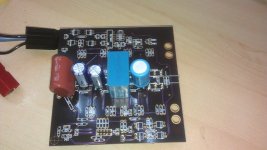
So in the zip file attached is my driver stage. It is based on a ST TD350E driver chip. I tried to incorporate reliability and fault detection into this, how well it works is yet to be seen. Highhopes has said he has had good experiences using this driver. This driver has been buffered to allow a gate drive of up to 14A peak current (2W power supplies instead of the 1W ones I am using would probably be needed to realize this level). The propagation delay of the entire setup should be ~500nS.
I have an open office document in the zip file that explains the basic circuit operation and what each component does, but I don't know if the part numbers exactly match up any more. I need to update it, so if you see something off, just ignore it or figure out what part number it's really referencing if you want to understand it. It was more for my own use than anything else to make sure I was understanding what I was doing.
In the zip file there is a PDF schematic of the driver section, low side and high side. Sub directories contain SVG images of the board layout sections, Gerber has the Gerber files and KiCad contains all the files that should be needed to open everything up in KiCad and look at it there.
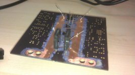
Comments are welcome, but I don't think I will be changing much unless a major error is found somewhere. Sorry my layout is so sloppy, I just haven't gone back to clean it up as much as it needs. The net naming was done they way it is in KiCad to allow me to have the routing I wanted without it giving me errors.
I am hoping to be able to get a maximum of 200A peak from this layout. Once I have things working as a 6 FET I will keep adding FETs until I'm at 24 FETs. Once I max that out then I'll make changes from what I learned and go to TO-247 FETs, I left enough room to be able to build an 18 FET controller with the same board space. Reliability and failure mode detection were thought of during the design, it's one of the reasons each high/low section utilizes it's own isolated supply (6 for the driver stages, 1 for the brain board, 1 from the battery to supply 24V to the isolated supplies) and the only electrical connection between high and low side is the phase output. Everything is then optically coupled back to the brain board (which I'm currently redesigning to incorporate a PIC processor I am using to handle error processing). I am hoping this minimizes the chances of me nuking Lebowskis processors.
Anyway, have at it, you won't hurt my feelings. I'm just some guy with a High School diploma diving into a complex project.
View attachment TD350 Driver.zip
So in the zip file attached is my driver stage. It is based on a ST TD350E driver chip. I tried to incorporate reliability and fault detection into this, how well it works is yet to be seen. Highhopes has said he has had good experiences using this driver. This driver has been buffered to allow a gate drive of up to 14A peak current (2W power supplies instead of the 1W ones I am using would probably be needed to realize this level). The propagation delay of the entire setup should be ~500nS.
I have an open office document in the zip file that explains the basic circuit operation and what each component does, but I don't know if the part numbers exactly match up any more. I need to update it, so if you see something off, just ignore it or figure out what part number it's really referencing if you want to understand it. It was more for my own use than anything else to make sure I was understanding what I was doing.
In the zip file there is a PDF schematic of the driver section, low side and high side. Sub directories contain SVG images of the board layout sections, Gerber has the Gerber files and KiCad contains all the files that should be needed to open everything up in KiCad and look at it there.
Comments are welcome, but I don't think I will be changing much unless a major error is found somewhere. Sorry my layout is so sloppy, I just haven't gone back to clean it up as much as it needs. The net naming was done they way it is in KiCad to allow me to have the routing I wanted without it giving me errors.
I am hoping to be able to get a maximum of 200A peak from this layout. Once I have things working as a 6 FET I will keep adding FETs until I'm at 24 FETs. Once I max that out then I'll make changes from what I learned and go to TO-247 FETs, I left enough room to be able to build an 18 FET controller with the same board space. Reliability and failure mode detection were thought of during the design, it's one of the reasons each high/low section utilizes it's own isolated supply (6 for the driver stages, 1 for the brain board, 1 from the battery to supply 24V to the isolated supplies) and the only electrical connection between high and low side is the phase output. Everything is then optically coupled back to the brain board (which I'm currently redesigning to incorporate a PIC processor I am using to handle error processing). I am hoping this minimizes the chances of me nuking Lebowskis processors.
Anyway, have at it, you won't hurt my feelings. I'm just some guy with a High School diploma diving into a complex project.
View attachment TD350 Driver.zip
")