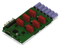
Serious FOCer (84V VESC 6 based controller)

To save space you can reroute mosfets so they are bolted down under the pcb to a case. In such a way case width will remain the same, but provide slimmer design with improved thermal management solution.
Do you plan to add BT module for Android/iOS app control?
 
Which model of controller are you referring to? The MOSFETs for the 6 FET models still allow them to be bolted to the wall of an enclosure. Very similar to how ebike controllers currently are and how people are familiar with. Are you suggesting that they be horizontally mounted underneath like in the BESC from @galp?

I'm leaving it to the user/company to add a generic bluetooth module of choice. I don't want to deal with FCC certifications for intentional radiators. One can just add a pre-certified module and be done.
 
Yes, in similar manner like BESC but with mosfets holes direction to a center of pcb. They can be bolted from outside of enclosure.
Any updates with review?
 
I would have to alter the layout and routing to accommodate the FETs in the orientation you are referring to. It would indeed save space on the Z axis. I will think about doing this.

I am still waiting for feedback from the reviewer(s). They are doing this for free in their spare time.
 
Got some initial feedback from Mr. Vedder.

He confirmed that the DRV8353 is more or less already supported in the firmware as I suspected.

He also verified that the low-side shunt resistors along with the integrated current sense amplifiers of the DRV8353 will work.

There may or may not be more feedback from him in the future. Either way, its good to have Mr. Vedder’s comments on my design.
 
Also I have contacted @marcos, one of the engineers who created the Axiom Controller, about hiring him to do a professional review of my controller design. This will help prevent issues before they happen. Thankfully I have received enough donations to cover half of his charges! This is great since he charges half up front to start the review.
 
Is this a 2 layer or 4 layer board? If 2 layer, I would seriously consider switching to 4 layer and remove those TH gate resistors. That's really not the place to use leaded (inductive) parts.
Switching from 2 to 4 layer will only add 5-10% cost on the PCB in volume production IIRC.
 
I'm not sure I'll be manufacturing in large enough quantities to justify 4 layers. For example a qoute from Bittele for 500 2-layer 2oz copper PCBs is $846. 4-layer is $1575. What volumes did you have in mind to achieve only a 5 to 10% cost difference?

You're right about the leaded gate resistors being inductive. I'll be discussing those with @marcos. The main reason behind those are to allow for more of the top layer copper to be used for the high-current switch node. It may not be worth it to do this after all.
 
depends how you look at it. i see a 1,5 dollar raise on a product of 50-100 dollar. that is only 1.5-3%

so you add 3% to the cost. but you add value in lower overshoot and more copper for the high power traces. if you can get away without beefing up the traces manually this will save a lot of labor and even lower the total cost of the product.
 
Ah yes I can see the cost difference would not be as large for the final cost of the unit rather than just comparing PCB prices.

Yes there are pros and cons for 2-layer. I do intend on offering DIY kits to individuals of which the customer does the assembly for the through hole components and wires. 4-layer would be better for DFM as it would reduce costs for fully assembled units. Thankfully nothing is set in stone yet. I have time to make adjustments as needed. Thankfully I'm going through a review process to catch any of my mistakes or non-ideal qualities before I produce units.
 
@nieles the more I think about a 4-layer PCB the more I think you're right. A 4-layer PCB will mean less noise, more copper, cooler board, better layout/routing, and easier/cheaper assembly. 4 layers of 2oz copper should be beefy enough on its own to handle the current.
 
its really a 'dificult' decision. as the answer is different depending on what you want to do, and your overall goal.

as for a DFM perspective, 4 layer would be a no-brainer for this project. but as you say this is more a DIY (or semi DIY) project. so you don't need to pay for hand labor for beefing up the traces

but then you need to consider warranty. do you give warranty on a product that the user needs to solder on them self?

you could go 1oz inner layer and 2oz outer layer. (more standard i think)

also make sure you have you copper balance in check with 2oz. as the warping forces will be greater.
 
You bring up some good points @nieles. Maybe I should have you review the design too!

This controller is meant to be a balance of DIY and DFM. The DIY kit should make the DIYers happy since they can solder some components themself and even choose which FETs to use if they wish. Yes figuring out a warranty for this type of thing may be difficult. I'll have to see what sort of warranties are available for other DIY electronics kits. A warranty is more of a business aspect.

I'll be consulting with John Teel from Predictable Designs next month to discuss the manufacturing and business aspects. Hopefully we can find answers for things like warranties, liabilities, manufacturing, ect.
 
well as soon as money exchanges hands you become more or less a business. as people expect certain things from you.
people will email you with (silly) questions. people not skilled enough will think they are, start the project and mess up. then come back to you with questions.

good you are consulting different people. as this will give you lots of different insights in all the aspects.

i am a hardware engineer for a company that designs and produces electronics for our clients (no own products)
so keep this is mind with my comments. this biases my comments, how we do things.

we outsource PCB/PCBA production. then we do testing / end assembly in house.
we generally only deal with 3rd line support.
 
4 layers has several benefits. I'm used to low volume runs and a good 2 layer layout takes like 10 times more than a good 4 layer layout, this is a win in both engineering cost and time to market. Its just simpler to route, and saves yourself headaches when you have to go through an EMC chamber.

I havent looked at this yet, but I imagine 4 layer will cost you an extra $3 or $4. If you are willing to spend $10 extra towards a higher quality product, $4 for the extra layers is where your money is best spent as it has an impact across every aspect of your design. More copper, denser component placement, better EMI, less design effort. Its like in a car, better tires is where you want to spend your first $, not mosfets.

In this case what really makes or breaks the product is the powerstage reliability, with focus in the gate driver. I'm keen to go through the layout and schematic, maybe for $0 to $6 in BOM cost increase we can make it last for 5 more years, or at least save shaman from angry customers and fires during testing!
 
I appreciate the in depth input! Seems like 4 layers is the winner here.

If I go to 4 layers then this will be my first 4-layer PCB. I actually put a lot of time into researching proper 2-layer routing and layout techniques but I'm ok with ditching that for something that's clearly better.
 
As mentioned above, don't underestimate the post sales support required. It can eat you alive. Then when you are overwhelmed, folks will start complaining about no timely response.

May I recommend that you set up a Message Board for your company. Have it up and running before sales start. Point people to that area to ask questions. That way others may chime in and help those with difficulties. Also it will become your defacto FAQ, where answering the question once will supply that solution forever more.

All the best with your endeavor. BTW, If you have power traces on all 4 layers, mind the power dissipation of the inner layers. Those submerged layers are very difficult to shed heat.
 
@bigmoose this is much appreciated wisdom.

Thankfully I have experience in customer support. The company I work for full time has a dedicated forum to handle questions and issues from the field. Questions can be anywhere from the hobbyist to a tier 1 customer like BMW. Part of my job is to handle questions for particular ICs from this forum. The answer could be a simple as pointing out a section of the datasheet or as involved as a 1 month long series of tests in the lab.

The VESC itself has its own forums that help mitigate questions from the field. It would be nice to have something similar for my own controller. Since it's VESC based, I wonder if I could piggy back off of existing forums where the community/customers already have a presence.

Yes the inner layers heat up much more hence why thier max current is around half the rating of outer layers. I'm hoping that good placement of thermal vias will help even out the heat of the layers.
 
With such component placement density with 2 layer only, low volume run is there a real need for 4 layer layout? If it's DIY, power traces can be beefed up manualy at not much cost. Inner layers can't be used for power stages as bigmoose advised.
Just a thought. If it's going to be open source diy, Shaman I guess business can't give you proper advice how to handle this project.
Regards.
 
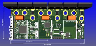
top.jpeg
TOP

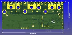
bottom.jpeg
BOTTOM

I’ve done most of the serious updates to the design. Check out the changes below.

  • Converted PCB to 4-layers
  • Added mounting holes (MH1, MH2, MH3)
  • Added pinouts for USB and unused MCU pins
  • Widened rings around cable through hole pads
  • Added fiducials (required for automated pick and place assembly)
  • Various routing improvements thanks to using 4 layers

I have also submitted the design files to @marcos for review. I look forward to his comments on this design!
 
peters said:
666 mils/FET. (=101.5mm/6/0.0254)
Are you sure?

Wow I would have never found that. Guess I'll have to toss this design entirely...
:wink:
 
d171beb09e7a9e8718cb0b590a0ac24f9ddac2da.jpeg

16d876c42275d8f2b8a5c632fa6e93b37b0165ca_2_1035x595.jpeg

adca25b4a5a30e954d404d4d59e226dfa12cbb00.jpeg
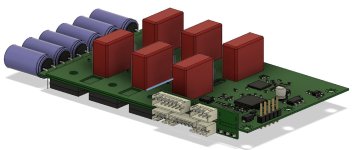
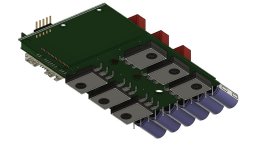
(models are a rough draft. Not finalized)

Big changes. Big gains. For those that donated, you’re getting your money’s worth. Overall height with enclosure is now estimated to be 18mm. Overall dimensions of Serious FOCer with enclosure is estimated to be 130mm x 70mm x 18mm. Estimated dimensions of Little FOCer with enclosure to be 100mm x 50mm x 18mm.

I’ve added 2 more hours of time with @marcos. It’s not free so anything you can toss my way helps me out. The more you and I invest, the better this product gets. @marcos, I'm getting closer to round 2 :)

Stay tuned. Things are getting Serious.
 
Back
Top